Photovoltaic Cutting Solutions

As photovoltaic production shifts toward thinner wafers and larger silicon ingots, manufacturers face rising pressure on yield, cost, and process stability. Our cutting solution combines optimized diamond wire, precise tension control, and proven process parameters to reduce kerf loss, increase wafer output, and minimize wire breakage. Designed for continuous, high-throughput production, it helps improve consistency, extend wire life, and deliver a more predictable cost per wafer.

Industry Challenges

The photovoltaic industry is shifting toward larger wafers (M10, G12) and thinner substrates — a combination that pushes conventional slicing to its limits.

Breakage Risk

Thin wafers are prone to edge chipping and micro-cracks.

TTV Control

Maintaining thickness uniformity on larger formats.

Wire Bow

Tension stability during extended cutting.

Material Loss

Kerf waste directly impacts ingot yield.

Our Methodology: Solving the Precision-to-Yield Equation

We don’t just provide equipment; we deliver a stabilized slicing process. In the transition to thinner wafers and larger formats, our methodology focuses on controlling the physical variables that dictate your final yield.

Stress-Controlled Slicing
As wafers thin to 100μm,, mechanical impact becomes the enemy. Our approach prioritizes precise feed-speed synchronization to minimize micro-cracks and edge chipping. By managing tension at the “initial bite,” we ensure structural integrity is never sacrificed for throughput.
TTV & Vibration Management
To solve Wire Bow issues in M10/G12 ingots, we implement high-frequency tension feedback. This stabilization keeps the wire path true, strictly controlling Total Thickness Variation (TTV) and achieving a surface finish of Ra≤0.2μm, reducing the burden on downstream texturing.
Kerf Loss & Yield Optimization
Reducing cost-per-watt starts with saving silicon. Our process logic optimizes the synergy between ultra-fine diamond wires and coolant fluid dynamics. By reducing friction-induced heat, we minimize kerf waste and maximize the number of high-quality wafers recovered from every ingot.
Thermal & Dimensional Stability
Precision requires thermal consistency. We manage the cutting zone temperature to prevent wire expansion and saw marks. This ensures tight dimensional accuracy ($\pm 0.1mm$), providing the flat, uniform substrates required for high-efficiency TOPCon and N-type cell lines.
Adaptive Process Feedback
We treat slicing as a closed-loop system. By analyzing wafer data—from warp to roughness—we provide an adaptive process window. This ensures consistent yields even when material grades vary or environmental conditions shift across different production shifts.

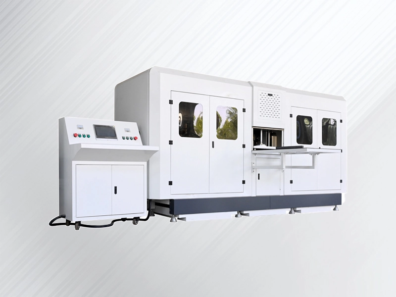
Targeted Cutting Solutions for Photovoltaic Materials

In the PV industry, the material defines the process. We provide specialized slicing and squaring logic designed to handle the unique physical properties of silicon, ensuring your production line achieves maximum yield with minimal kerf loss.

Silicon Ingot Squaring & Bricking

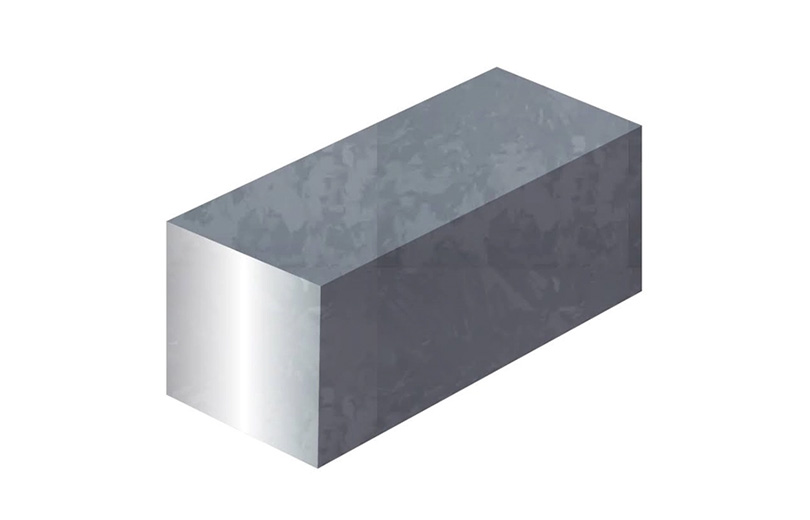
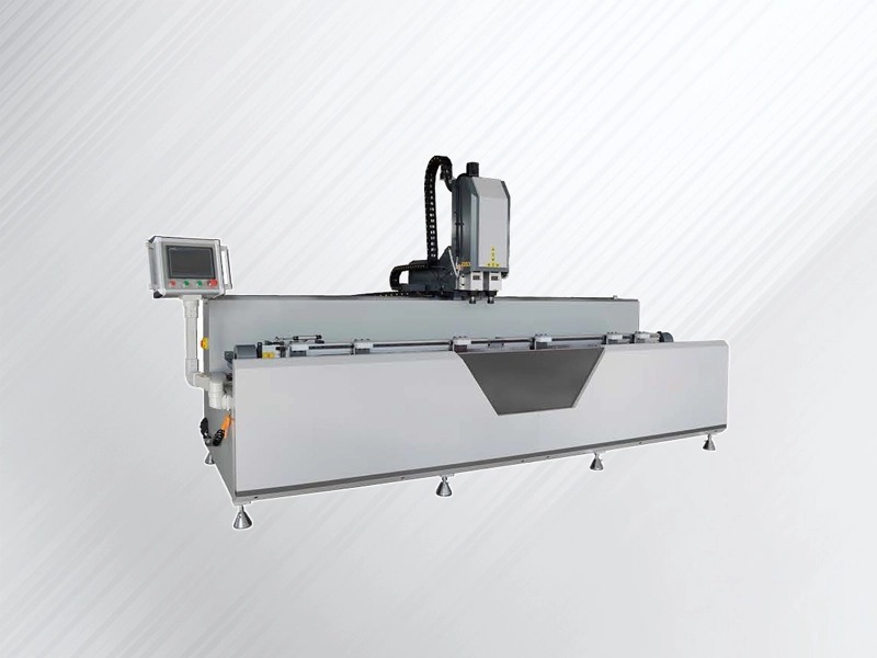
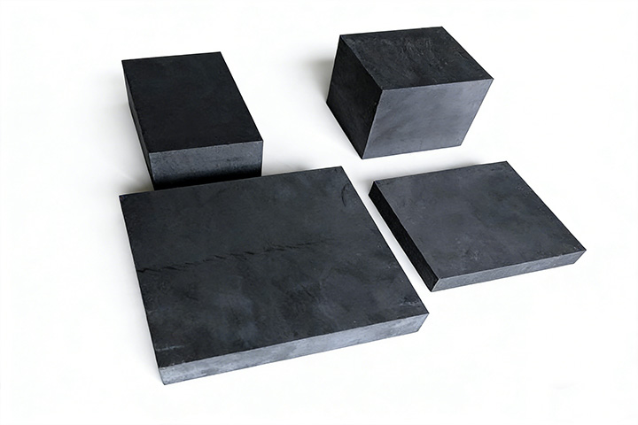
The journey to a high-efficiency cell starts with the Silicon Ingot. Our solution for ingot preparation focuses on geometric precision and surface integrity.

  • The Logic: By optimizing the diamond wire path during squaring, we ensure perfectly perpendicular faces and high dimensional accuracy (±0.1mm).

  • The Benefit: This precision reduces the material allowance needed for the next stage, maximizing the usable volume of the ingot and ensuring a stable foundation for high-speed wafering.

High-Yield Single-Crystal Silicon Slicing

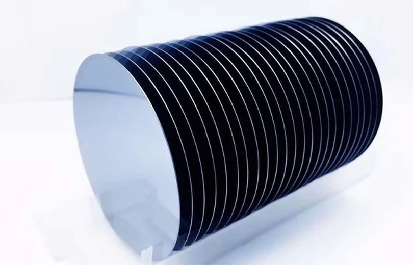
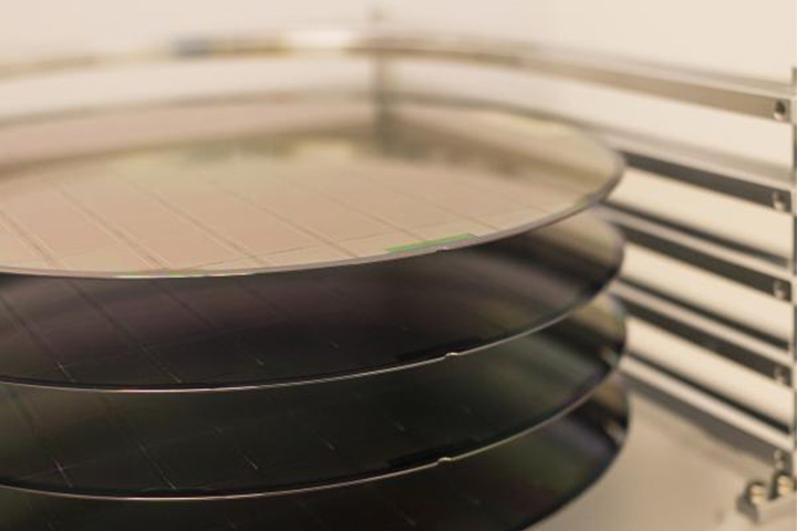
Single-crystal silicon is the backbone of high-efficiency N-type and TOPCon cells, but its brittle nature makes it prone to breakage during thin-wafer slicing.

  • The Logic: Our methodology centers on vibration-dampened slicing. We synchronize wire tension with adaptive feed rates to handle the transition to 100μm wafers.

  • The Benefit: By minimizing the mechanical stress on the crystal lattice, we significantly reduce micro-cracks and edge chipping, directly improving your final “A-grade” wafer yield.

Surface Engineering for Solar Cell Materials

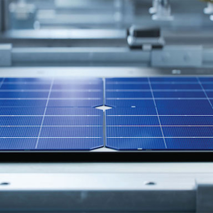
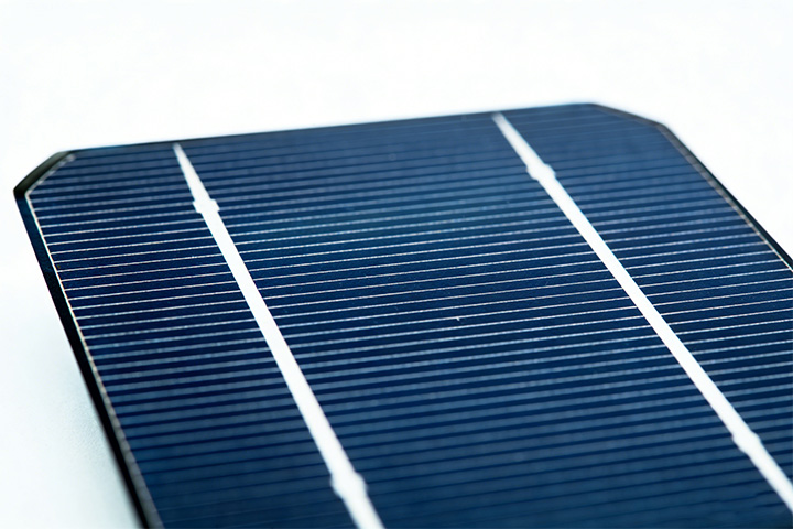
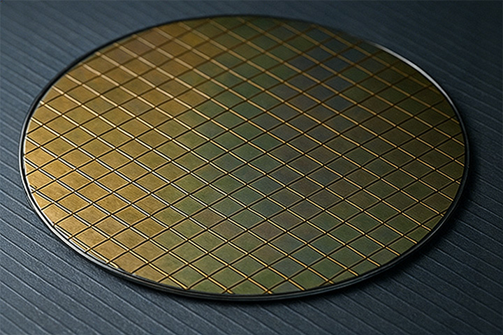
The quality of a Solar Cell Material isn’t just about its thickness; it’s about the texture left behind by the cut. Downstream texturing and etching processes require a uniform surface.

  • The Logic: We utilize a controlled cooling and lubrication process to manage the friction between the diamond wire and the silicon. This prevents “saw marks” and maintains a consistent surface roughness of Ra≤0.2μm.

  • The Benefit: A smoother, more uniform surface simplifies the chemical treatment in cell manufacturing, leading to better light-trapping capabilities and higher conversion efficiency.

Scalable Solutions for Large-Format Photovoltaics

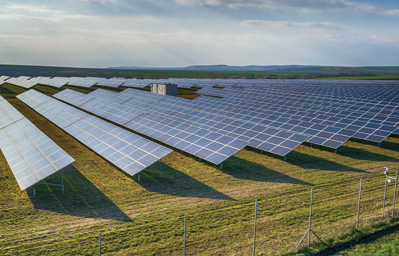
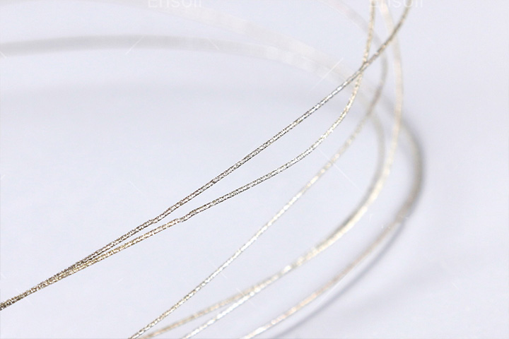
The industry shift toward M10 and G12 formats introduces significant “Wire Bow” challenges due to the longer cutting paths.

  • The Logic: For these large-format Photovoltaic substrates, our solution implements a high-frequency tension compensation loop. This keeps the wire taut and straight across the entire width of the ingot, even during high-linear-speed operation.

  • The Benefit: This stabilizes the TTV (Total Thickness Variation) across the large surface area, ensuring that every wafer—from the edge to the center—meets the strict tolerances required by automated module assembly lines.
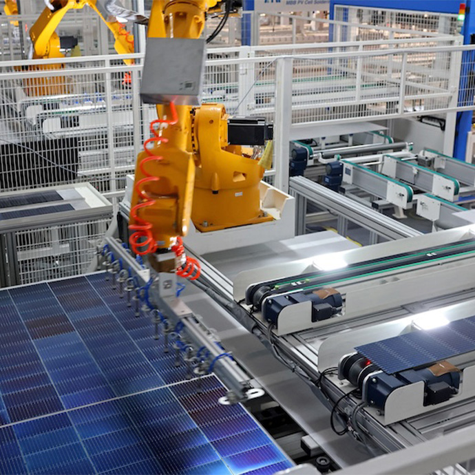
Production Workflow

A stabilized, controlled slicing process optimized for high-yield silicon wafer production.

1

Ingot Preparation

Material inspection for internal stress to ensure stability during ultra-thin slicing.
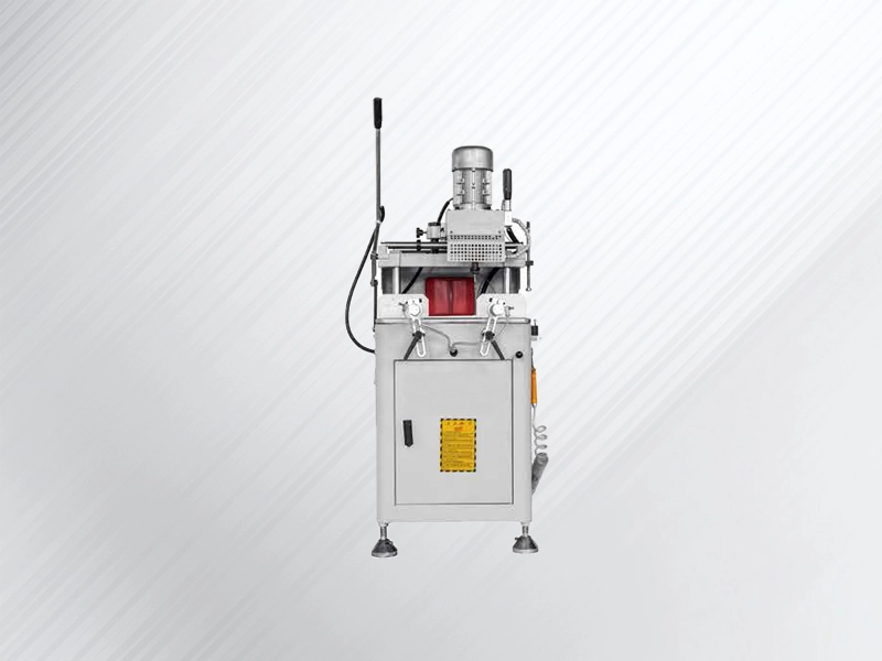
2

Squaring & Bricking

Defining geometric foundation with dimensional accuracy of ±0.1mm.

3

Mounting & Alignment

Synchronizing high-frequency tension feedback with feed rates to mitigate micro-cracks.

4

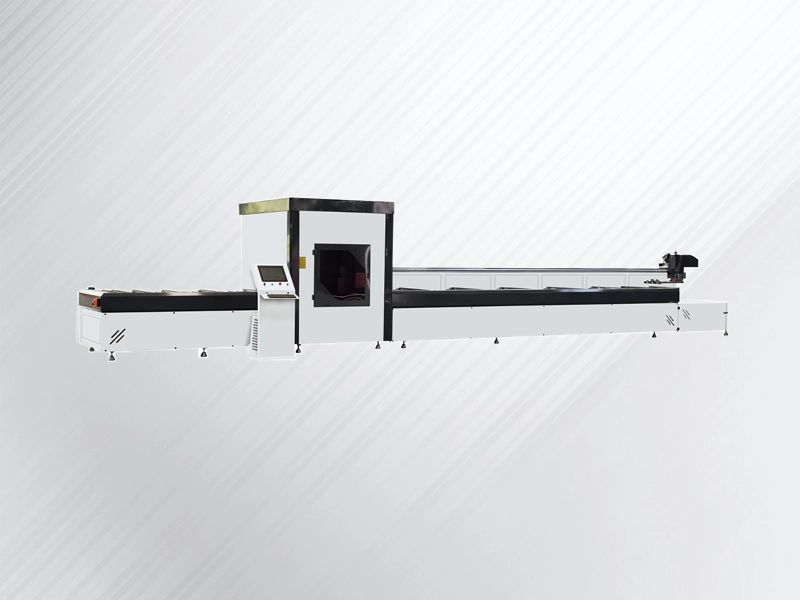
High-Efficiency Slicing

Vibration-managed process for 100μm – 130μm wafers with Ra ≤ 0.2μm surface.

5

Cleaning & Inspection

Automated ultrasonic cleaning and TTV/Warp verification for “A-grade” substrates.

Application

Why Choose Zelatec

Deep Industry Experience
Zelatec has extensive experience in precision cutting for hard and brittle materials, including silicon used in photovoltaic applications. Our team understands the unique demands of solar wafer production and the technical hurdles that can affect yield and cost.
Customized Cutting Strategies
Instead of offering one‑size‑fits‑all equipment, we work with customers to design and refine cutting processes tailored to their specific materials and production goals. This includes guidance on optimal wire tension, feed rates, and coolant strategies to balance quality and throughput.
Rigorous Quality Assurance
Every tool and component we supply undergoes strict testing, including tension checks and microscopic inspections, to ensure consistent performance. This commitment to quality helps reduce unexpected downtime and supports more reliable production outcomes.
Bespoke Engineering Support
We offer tailored customization—from diamond coating patterns to wire configurations and loop sizes—so your cutting system matches your material and machine requirements precisely.
Comprehensive Technical Support
Our engineers provide practical, remote technical support, including process optimization guidance, troubleshooting, and operational advice. This ensures your team can maintain stable operations and achieve the best possible results from your cutting setup, no matter where your facility is located.
Customer‑Focused Partnership
We aim to build long‑term relationships by understanding your challenges, delivering measurable results, and supporting your production goals with practical solutions—not just products.

Related Products

Related Solutions

Request a
Free Consultation