Silicon wafers are cut through a series of precision processes that typically include silicon crystal growth, ingot preparation, wafer slicing, edge processing, and, later in semiconductor manufacturing, wafer dicing.
Although silicon is one of the most important materials in modern electronics, it is also hard and brittle. This combination makes precision processing challenging. Excessive cutting force, poor process control, or unsuitable cutting parameters can lead to micro-cracks, edge chipping, material loss, and surface damage.
Another important point is that silicon wafer cutting does not refer to just one process. Different stages of semiconductor manufacturing require different cutting technologies. A silicon ingot must first be sliced into thin wafers. Later, after semiconductor devices have been manufactured on the wafer, the wafer is divided into individual dies.
This guide explains how silicon moves from a crystal ingot to precision wafers and how finished wafers are later diced into individual semiconductor chips. It also compares the main silicon wafer cutting methods, explains the challenges involved, and looks at the role of diamond wire cutting in processing hard and brittle materials.
From Raw Silicon to a Crystal Ingot
Before silicon can be cut into wafers, it must first be converted into a highly controlled crystalline form.
Raw silicon is refined to achieve the purity required for semiconductor or photovoltaic applications. The silicon is then processed to form a crystal with a controlled structure. This crystal is eventually formed into a silicon ingot, which becomes the starting material for wafer production.
The crystal structure is important because many semiconductor properties depend on the quality and orientation of the silicon crystal. For this reason, silicon wafer production begins long before the cutting stage.
The general process can be summarized as:
High-purity silicon → Crystal growth → Silicon ingot → Ingot preparation → Wafer slicing → Surface processing → Finished silicon wafer
For wafer manufacturers, the cutting stage is one part of a larger manufacturing chain. However, it is a particularly important step because it affects material yield, wafer thickness, surface condition, and the amount of additional processing required.
Why Silicon Must Be Crystallized
A silicon wafer used in semiconductor manufacturing normally requires a carefully controlled crystalline structure. Simply casting silicon into an arbitrary shape is not sufficient for many high-performance applications.
Crystal growth makes it possible to produce silicon with controlled characteristics. The resulting crystal can then be processed into a cylindrical ingot and sliced into wafers.
Two important crystal growth methods are commonly associated with high-quality silicon production: the Czochralski process and the Float Zone process.
Silicon Crystal Growth Methods
Czochralski (CZ) Process
The Czochralski process is one of the best-known methods for producing single-crystal silicon.
In simplified terms, a seed crystal is brought into contact with molten silicon and carefully pulled upward while rotating. Under controlled conditions, silicon solidifies around the seed crystal and forms a large cylindrical single-crystal ingot.
The CZ process is widely associated with the production of single-crystal silicon for semiconductor applications. After the crystal growth stage, the ingot can be processed to achieve the required diameter, orientation, and surface condition before wafer slicing begins.
Float Zone (FZ) Process
The Float Zone process is another method used to produce high-purity single-crystal silicon.
Rather than relying on a conventional crucible during the main crystal growth stage, the process uses a controlled molten zone that moves through the silicon material. This approach can help reduce certain impurities and is used for applications where very high material purity and specific electrical properties are required.
Although CZ and FZ silicon differ in their production routes and typical applications, both methods ultimately produce silicon material that can be processed into wafers.
For a cutting process, the important point is that the ingot must be properly prepared before precision slicing begins.
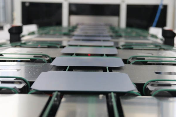
Preparing Silicon Ingots for Wafer Cutting
A silicon ingot cannot simply be placed into a cutting machine immediately after crystal growth. Several preparation steps may be required to improve cutting stability and ensure that the resulting wafers meet dimensional and quality requirements.
Typical preparation operations include:
Ingot Shaping
The ingot is processed to achieve the required geometry. Cylindrical silicon ingots may undergo shaping operations before slicing.
Diameter Grinding
Grinding can be used to achieve a more consistent diameter and improve the outer geometry of the ingot. A stable and uniform ingot shape helps support consistent cutting.
Crystal Orientation
The crystal orientation may be identified and controlled according to the intended wafer specification. The orientation can influence how the material is processed and used in later semiconductor manufacturing steps.
Surface Preparation
The ingot surface may be prepared to remove irregularities and improve handling during subsequent processing.
Ingot Inspection
Before slicing, the ingot may be inspected for dimensional accuracy and material quality.
Proper ingot preparation helps improve slicing stability and wafer quality. Even an advanced cutting system cannot completely compensate for problems caused by poor material preparation.
How Are Silicon Wafers Actually Cut?
Silicon wafers are primarily produced by slicing a silicon ingot into thin sections using precision cutting technologies, particularly wire-based cutting systems.
The exact cutting method depends on factors such as:
- Silicon type
- Ingot diameter
- Required wafer thickness
- Production volume
- Material cost
- Surface quality requirements
- Acceptable kerf loss
- Downstream processing requirements
Historically and technologically, several methods have been used for silicon wafer slicing. The most relevant methods include wire slicing, ID sawing, and multi-wire sawing.
Main Silicon Wafer Slicing Methods
Wire Slicing
Wire slicing uses a moving wire to gradually remove material from the silicon ingot.
Depending on the process, the cutting action may involve abrasive particles associated with the wire system. The wire moves through the cutting zone under controlled tension and speed while the silicon material is gradually separated.
Wire-based cutting offers several advantages for hard and brittle materials because the cutting force can be distributed over a relatively small and controlled cutting area.
Important process factors include:
- Wire speed
- Wire tension
- Feed rate
- Wire diameter
- Abrasive characteristics
- Cooling and process conditions
Wire slicing is particularly important in applications where material utilization and cutting precision are important.
ID Sawing
ID sawing uses an Internal Diameter saw, in which the cutting edge is located on the inner diameter of a circular blade.
The silicon material is positioned and fed into the cutting area. ID sawing has been used as a traditional wafer slicing method and can provide controlled cutting for certain applications.
However, the process has limitations compared with modern high-throughput wire-based systems, particularly when manufacturers need to process large volumes of wafers efficiently.
For this reason, wire-based technologies have become increasingly important in applications that require high productivity and reduced material waste.
Multi-Wire Sawing
Multi-wire sawing uses multiple wire sections to cut through a silicon ingot simultaneously.
Instead of producing one wafer at a time, the system can process multiple slices in parallel. This makes multi-wire sawing especially important for high-volume manufacturing environments.
The technology is associated with applications where manufacturers need:
- High throughput
- Consistent wafer production
- Efficient use of cutting equipment
- Repeatable wafer thickness
Multi-wire sawing has become important for applications requiring high throughput and consistent wafer production, particularly in semiconductor and photovoltaic manufacturing.
Diamond Wire Cutting
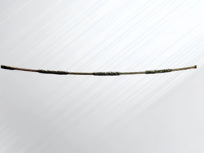
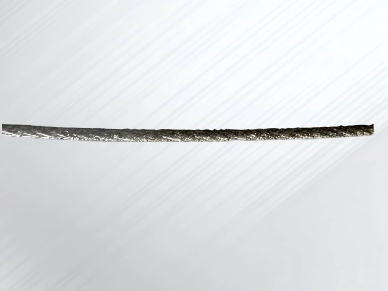
Diamond wire cutting uses a wire with diamond abrasive particles to remove material from the workpiece.
Because diamond is extremely hard, diamond-coated wire can be used for cutting hard and brittle materials, including silicon and other advanced materials.
The potential advantages of diamond wire cutting include:
- Narrow cutting kerf
- Reduced material loss
- Controlled cutting forces
- Precision material removal
- Reduced mechanical stress compared with some conventional cutting approaches
- Suitability for hard and brittle materials
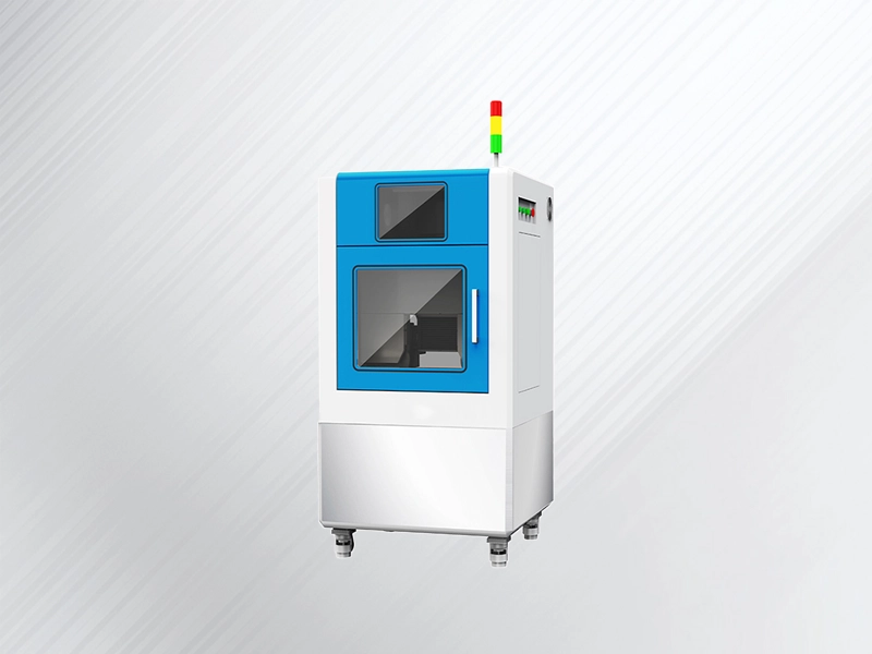
The cutting process depends on the complete system rather than the machine alone. Machine stability, wire characteristics, cutting speed, feed rate, and material properties can all influence the final result.
For silicon ingot slicing and other precision applications, diamond wire cutting can be selected when the application requires precise material removal, controlled cutting forces, and efficient processing of hard and brittle materials.
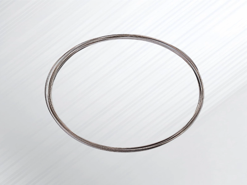
For equipment manufacturers and processors, this is where a dedicated Diamond Wire Cutting Machine and the correct Diamond Wire Loop or wire configuration become important parts of the overall process.
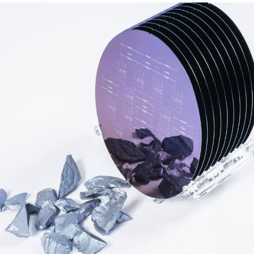
The Main Challenges of Silicon Wafer Slicing
Silicon wafer slicing is not simply about separating material. The process must also control damage and material loss.
Kerf Loss
Kerf loss refers to the material removed by the cutting process.
Silicon is a valuable material, and the material converted into cutting debris cannot become part of the finished wafer. Therefore, reducing unnecessary kerf loss can improve material utilization.
Wire diameter, cutting technology, and process parameters can all influence the amount of material lost during slicing.
Micro-Cracks
Silicon is brittle, which means localized stress can create small cracks.
Micro-cracks may not always be obvious immediately after cutting, but surface and subsurface damage can affect later processing steps. Careful control of the cutting process is therefore important.
Edge Chipping
Chipping can occur when small pieces break away from the edge of the silicon during cutting or handling.
The risk of edge damage depends on material properties, cutting conditions, and the stability of the workpiece.
Thickness Variation
A silicon wafer must often meet strict thickness requirements. Variations in cutting conditions can produce differences across the wafer.
Machine rigidity, wire stability, feed control, and material preparation all affect thickness consistency.
Surface Damage
The slicing process can leave a damaged surface layer that requires further processing.
Grinding, lapping, and polishing may be used to improve the final surface condition.
Wire Wear
The cutting wire is a critical process component. As the wire is used, its cutting characteristics may change.
Wire construction, abrasive quality, coating condition, and operating parameters can affect cutting consistency and tool life.
Understanding these challenges helps manufacturers choose a cutting method that balances productivity, material yield, and quality requirements.
Post-Slicing Silicon Wafer Processing
Cutting does not produce a finished semiconductor wafer by itself. Additional processes are usually required to achieve the required thickness, surface condition, edge quality, and cleanliness.
Edge Processing
Wafer edges may be processed to improve their geometry and reduce the risk of damage during handling.
Edge shaping can help reduce stress concentrations that may contribute to chipping or cracking.
Surface Grinding
Grinding may be used to improve wafer thickness control and remove part of the surface damage created during earlier processing.
Lapping
Lapping can further improve flatness and surface condition.
Polishing
Polishing is used when a smoother surface is required. Semiconductor wafers may undergo highly controlled polishing processes before device manufacturing.
Cleaning
Particles and process residues must be removed before subsequent manufacturing stages.
Inspection
Finished or semi-finished wafers may be inspected for:
- Thickness
- Surface condition
- Flatness
- Edge quality
- Defects
- Particle contamination
These post-slicing processes demonstrate why silicon wafer manufacturing should be understood as a complete precision-processing chain rather than a single cutting operation.
What Is Silicon Wafer Dicing?
Wafer slicing and wafer dicing are different processes.
Wafer slicing produces wafers from a silicon ingot, while wafer dicing separates a processed wafer into individual semiconductor dies.
This distinction is essential.
During slicing, the starting material is typically a silicon ingot.
During dicing, the starting material is already a processed wafer that may contain multiple semiconductor devices. The purpose is to separate those devices into individual chips.
Because the objectives are different, the technologies used can also be different.
Main Silicon Wafer Dicing Methods
Blade Dicing
Blade dicing is an established mechanical method for separating semiconductor wafers.
A thin diamond blade cuts along predetermined dicing streets to separate the wafer into individual dies.
Blade dicing remains widely recognized because it is a mature and well-understood technology.
However, mechanical contact can create challenges, particularly for delicate or brittle materials. Process optimization is necessary to control chipping and mechanical damage.
Laser Dicing
Laser dicing uses a focused laser beam to process the wafer.
Because the laser does not require direct mechanical contact with the cutting surface, laser-based processes can be useful for precision applications.
However, thermal effects must be considered. Depending on the laser technology and process conditions, heat can influence the surrounding material.
Different laser approaches may be selected depending on wafer thickness, material properties, and precision requirements.
Plasma Dicing
Plasma dicing uses plasma-based material removal to separate individual dies.
The process can be suitable for thin and delicate wafer applications because it avoids direct mechanical blade contact.
However, plasma dicing is a specialized process that requires dedicated equipment and carefully controlled manufacturing conditions.
Stealth Dicing
Stealth dicing uses laser energy focused within the wafer material to create an internal modified layer.
The wafer can then be separated along the modified region using a controlled process.
This approach can be useful where minimizing certain types of surface damage is important.
Cleaving
Cleaving uses the crystalline structure of the material to support controlled fracture.
Because silicon is a crystalline material, its structure can influence how it separates under controlled conditions.
Cleaving is a different approach from conventional cutting because the process relies more directly on controlled fracture behavior.
Wafer Slicing vs Wafer Dicing
The following table summarizes the main difference:
| Process | Starting Material | Main Purpose | Typical Methods |
|---|---|---|---|
| Wafer Slicing | Silicon Ingot | Produce individual silicon wafers | Wire sawing, diamond wire cutting, multi-wire sawing, ID sawing |
| Wafer Dicing | Processed Silicon Wafer | Produce individual semiconductor dies | Blade dicing, laser dicing, plasma dicing, stealth dicing |
This distinction is useful for both engineers and buyers because the equipment required for ingot slicing may be very different from the equipment required for semiconductor die separation.
How to Choose the Right Silicon Cutting Method
There is no single cutting method that is ideal for every silicon processing application.
The appropriate technology depends on several factors.
Material Type
Different silicon materials and advanced semiconductor materials can have different processing characteristics.
Hard and brittle materials may require cutting methods that provide controlled material removal and reduced mechanical stress.
Wafer or Workpiece Thickness
The thickness of the starting material can influence the choice of cutting technology.
Processes suitable for bulk ingot slicing may not be suitable for extremely thin finished wafers.
Required Precision
Applications with demanding dimensional tolerances may require more advanced process control.
Production Volume
High-volume manufacturing often requires equipment capable of producing consistent results over long production runs.
Multi-wire systems may be attractive for high-throughput applications, while other systems may be more appropriate for specialized or smaller-scale processing.
Surface Quality
If the cutting process creates significant surface damage, additional downstream processing may be required.
The overall production decision should consider both the cutting stage and the finishing work required afterward.
Kerf Loss
For expensive materials, reducing unnecessary material loss can be an important consideration.
Processing Speed
Higher speed is not always better if it compromises wafer quality. Manufacturers must balance productivity with cutting accuracy and material yield.
For silicon ingot slicing and hard, brittle material cutting, wire-based and diamond wire cutting technologies may be considered depending on the application.
The Role of Diamond Wire in Silicon Processing
The wire itself is an important part of the cutting system, as its construction and abrasive characteristics influence cutting performance.
Important factors can include:
Wire Diameter
A thinner wire may help reduce the width of the cutting kerf, although wire selection must also consider strength and process stability.
Diamond Abrasive
Diamond particles provide the cutting action. Their characteristics can influence cutting efficiency and surface quality.
Cutting Speed
The movement speed of the wire affects the interaction between the abrasive and the silicon material.
Material Compatibility
Wire configuration should be selected according to the material being processed and the required cutting result.
Wire Configuration
Different cutting machines may use different wire arrangements. Endless wire configurations can provide continuous cutting movement in appropriate machine designs.
For manufacturers processing silicon and other hard materials, the relationship between the cutting machine and the cutting wire should be considered as a complete system.
A Diamond Wire Loop, for example, is not simply a replacement component. Its construction, abrasive coating, and operating characteristics can directly influence the performance of the cutting process.
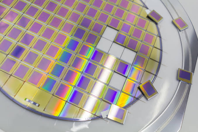
The Future of Silicon Wafer Cutting
Silicon wafer manufacturing continues to face pressure to improve material efficiency, precision, and production consistency.
Several broad trends are likely to remain important.
Thinner Wafers
As applications demand thinner semiconductor and photovoltaic materials, cutting and handling processes must provide greater control.
Larger Wafer Diameters
Larger substrates require stable equipment and consistent processing across a greater cutting area.
Reduced Kerf Loss
Improving material utilization remains important because reducing unnecessary cutting loss can improve manufacturing efficiency.
Higher Automation
Automation can help improve repeatability, reduce manual handling, and support more consistent production processes.
Improved Process Monitoring
Manufacturers increasingly rely on monitoring and control systems to identify changes in cutting performance and maintain process stability.
Advanced Semiconductor Materials
In addition to silicon, manufacturers are processing increasingly challenging materials such as silicon carbide, sapphire, ceramics, and other hard and brittle materials.
These trends increase the importance of precision cutting technologies and carefully selected cutting consumables.
Conclusion
Silicon wafer production involves far more than simply cutting silicon.
The process begins with high-purity silicon and controlled crystal growth. The resulting crystal is formed into a silicon ingot, prepared for processing, and then sliced into thin wafers using precision cutting technologies.
Wire slicing, ID sawing, multi-wire sawing, and diamond wire cutting can all play roles in silicon processing, depending on the application.
After slicing, the wafer may require edge processing, grinding, lapping, polishing, cleaning, and inspection before it reaches the required quality.
Later in semiconductor manufacturing, wafer dicing performs a separate function by dividing a finished wafer into individual semiconductor dies. Blade dicing, laser dicing, plasma dicing, stealth dicing, and cleaving each offer different approaches for this stage.
For hard and brittle material cutting applications, diamond wire cutting systems provide one possible approach for precision processing. When evaluating a cutting solution, manufacturers should consider the complete system, including the material, required precision, production volume, cutting method, machine configuration, and diamond wire characteristics.
For related applications, you can explore Diamond Wire Cutting Machines, Diamond Wire Loops, and silicon wafer cutting solutions designed for precision processing of hard and brittle materials.
FAQs on Silicon Wafer Cutting
How are silicon wafers cut?
Silicon wafers are primarily produced by slicing silicon ingots into thin sections using precision cutting technologies such as wire sawing and multi-wire sawing. Diamond wire cutting may also be used for precision processing of hard and brittle silicon materials.
What is the difference between wafer slicing and wafer dicing?
Wafer slicing cuts a silicon ingot into individual silicon wafers. Wafer dicing is a later process that separates a processed wafer into individual semiconductor dies or chips.
What is multi-wire sawing?
Multi-wire sawing uses multiple wire sections to cut a silicon ingot into many wafers simultaneously. It is widely associated with applications requiring high throughput and consistent wafer production.
Why is silicon difficult to cut?
Silicon is hard and brittle. Cutting forces can create micro-cracks, edge chipping, surface damage, and material loss if the process is not properly controlled.
What causes kerf loss during wafer cutting?
Kerf loss occurs because material is removed by the cutting process. Wire diameter, cutting method, and process parameters can influence the amount of silicon lost during slicing.
What is diamond wire cutting?
Diamond wire cutting uses a wire with diamond abrasive particles to gradually remove material. It can be used for precision cutting of hard and brittle materials, including silicon.
How thin can silicon wafers be cut?
The achievable thickness depends on the silicon material, cutting technology, equipment configuration, and downstream processing requirements. Very thin wafers generally require more careful control of cutting, handling, and post-processing.
What cutting method is used for semiconductor wafers?
Different stages use different methods. Silicon ingots are commonly sliced using wire-based technologies, while finished semiconductor wafers may be diced using blade, laser, plasma, stealth dicing, or other specialized technologies.
How can chipping and micro-cracks be reduced during silicon cutting?
Reducing chipping and micro-cracks generally requires appropriate cutting parameters, stable equipment, suitable cutting tools or wires, controlled feed rates, and proper post-processing.
Why is diamond wire important in silicon processing?
The characteristics of the diamond wire can influence cutting efficiency, kerf width, surface quality, and overall process stability. Wire diameter, abrasive properties, and configuration should therefore be selected together with the cutting machine and application requirements.