What Is Kerf Loss and Why It Matters
“Kerf” is the width of the cut made by a saw; kerf loss is the material removed (and thus wasted) during slicing. In wafer production, kerf loss can be enormous – typically 45–50% of silicon feedstock becomes wafer, while roughly 40% can be lost as slurry or wire-cut kerf waste. In other words, nearly half the ingot may be wasted, so even small kerf reductions significantly increase usable yield. For example, fixed diamond-wire sawing can achieve kerf widths as low as ~120–150 µm (micrometers), versus ~180–220 µm in conventional slurry multi-wire sawing. Reducing kerf from 220 µm to 150 µm for 180 µm wafers could boost wafer count by ~20%. In cost-sensitive industries (PV cells, IC chips, LEDs, etc.), recovering just 1–2% more material is worth substantial money.
Kerf loss also affects wafer quality: variations in kerf cause thickness non-uniformity and edge defects, raising scrap rates. Thus, controlling kerf ensures both higher yield and better wafer integrity. Modern diamond-wire machines routinely achieve sub-0.2 mm kerf widths. We discuss how to target and maintain these benchmarks.

Causes of Kerf Loss
Kerf loss arises whenever cutting removes material. Key factors include:
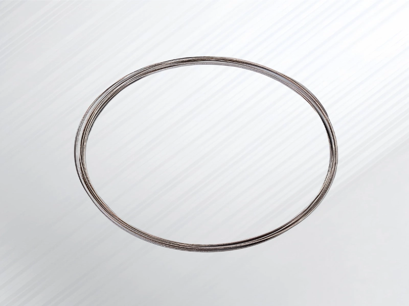
- Wire and Abrasive Characteristics: Wire type and size directly set the minimum kerf. Diamond-wire saws use fixed-abrasive thin steel wires. A thinner wire yields a narrower cut, but is more prone to vibration and heat buildup. Fixed-abrasive (diamond) wires cut with minimal kerf compared to free-abrasive slurry saws. For example, DWS (“fixed wire”) produces a more uniform, narrow kerf than loose SiC slurry wire sawing. Diamond grit size also affects cutting efficiency: very coarse grit can increase kerf by making larger chips.
- Wire Tension and Bow: Insufficient tension lets the wire bow, increasing effective kerf width. Higher tension straightens the wire (reducing lateral deflection) and lowers kerf loss. Conversely, if wire span (distance between guides) is too long or tension too low, lateral vibration amplifies and “excess” kerf is cut.
- Feed Rate: Pushing the wafer into the wire too fast can cause wire deflection and vibration, enlarging the kerf. Slower, more controlled feed reduces bow and improves stability. (Balancing feed vs. throughput is key – later sections detail optimal settings.)
- Wire Speed: Very high wire speed increases cutting power (force×speed) and heat, which can cause wire bow and thermal expansion in the slice. Research shows slightly higher speed “slightly increases” kerf loss. However, speed also improves material removal and can reduce subsurface damage. In practice, speed is optimized along with feed to balance productivity vs kerf.
- Material and Hardness: Hard, brittle materials (SiC, sapphire, GaN, technical ceramics) are more prone to chipping and wire-induced damage. Such materials often require more abrasive action, which can widen the kerf and cause microcracks. In contrast, softer materials (glass, some semiconductors) cut more cleanly. Material crystal orientation and toughness affect how the wire plows through: e.g., sapphire wafers (C-plane) exhibit more warping and kerf distortion if parameters aren’t tuned.
- Temperature and Coolant: Friction during cutting generates heat. In a narrow kerf, heat dissipation is limited. Localized heating causes thermal expansion in the wafer, increasing bow and “effective” kerf width. Poor coolant flow exacerbates this – insufficient cooling leads to softened material, larger chips, or glazed abrasives. Maintaining constant, clean coolant flow is essential.
- Machine Accuracy and Fixturing: Errors in machine calibration (guide alignment, wire pulleys, linear stages) cause uneven tension or unintended wire bow, increasing kerf. Loose fixturing or warped chucks can let the wafer shift or vibrate during cut, again enlarging the cut zone. Even thermal expansion of machine frames under load can affect kerf uniformity. High-precision motion systems (closed-loop servos, rigid frames) minimize these issues.
- Wire Wear and Condition: As the wire cuts, diamonds can pull out or become dull, which can actually change kerf profile over time. A worn wire can wander or skip, effectively widening or unevenly widening the kerf. Regular monitoring of wire life is needed.
- Other Factors: Vibration from external sources, loose machine foundations, or mechanical resonances can feed into the wire. Also, cutting multiple slices in one pass (multi-wire loops) can induce interactions between adjacent wires if chips aren’t flushed well, affecting kerf uniformity.
In summary, kerf width is determined by wire diameter, abrasive grit, and how the wire is used (tension/speed/feed). Secondary factors (machine, coolant, fixturing) modulate these primary causes. Understanding these lets us set quantitative targets next.
Quantitative Benchmarks and Targets
- Typical Kerf Width: Modern fixed-diamond wire saws achieve kerf widths on the order of 100–200 µm. For example, Zelatec’s data reports ~120–150 µm kerf on silicon wafers, compared to 180–220 µm for slurry saws. Sapphire and SiC saws often use slightly thicker wires (200–300 µm), so their kerf might be a few tens of microns larger, but similarly scaled by wire dia + 10–20 µm. In general, the minimum kerf is roughly wire diameter + 10–20 µm (one study shows sapphire kerf ≈ wire dia + 20 µm).
- Acceptable Yield (%): In high-end wafer production, every percent of yield is valuable. Typical crystalline silicon wafer lines aim for >50% wafer yield from the ingot, with <10–15% loss due to slicing (excluding block trim) as a stretch goal. In practice, combined kerf and edge trim losses can exceed 30–40% without tight control. Targets like reducing kerf loss to <1% of block volume are ambitious but can be approached with very thin wire and optimized process. When using fixed diamond wire, kerf loss can often be limited to 1–2% of feedstock (depending on wafer thickness) vs 4–8% for slurry sawing.
- Surface Roughness and Damage: While not kerf per se, wafer surface quality is often specified together with kerf: diamond-wire cuts routinely achieve as-cut surface roughness Ra in the 0.1–0.2 µm range. Post-etch/polish, advanced nodes demand sub-nanometer roughness (e.g. ~0.15 nm Ra). Total Thickness Variation (TTV) after slicing should be within tens of microns (e.g. <15 µm for 8-inch wafers). These numbers underscore the need to minimize kerf variation – uneven kerf leads to wafer thickness deviation and warpage.
In practice, set benchmarks like: kerf width ≤200 µm, consistency ±10 µm across the cut, TTV below spec (e.g. <20 µm), and wafer flatness within tens of microns. Exceeding these indicates excessive kerf or vibration.

Mitigation Measures (Step-by-Step)
1. Wire Selection and Preparation
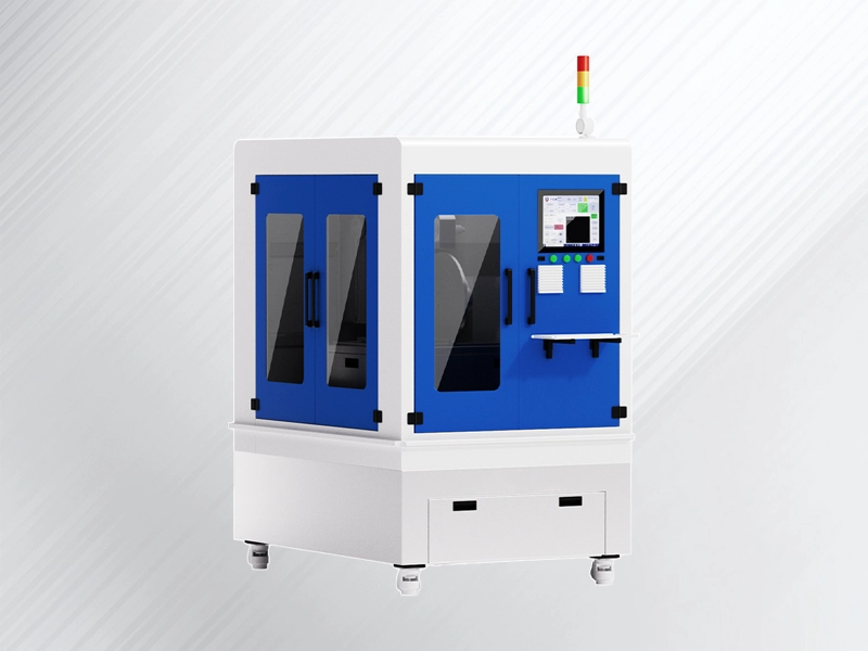
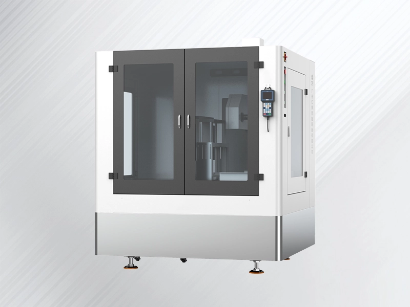
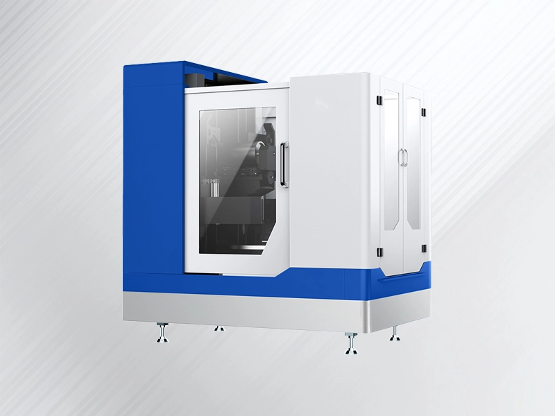
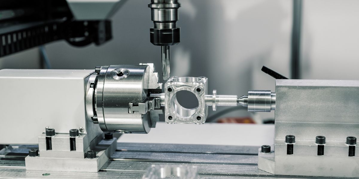
- Wire Type: Use high-quality fixed-abrasive diamond wire loops or plates designed for the material. For silicon and common semiconductors, electroplated or resin-bonded diamond wire is standard. For specialty substrates (e.g. KDP, sapphire), specialized wire coatings may help. The absence of loose abrasives (as in slurry) inherently reduces kerf – fixed wires cut more uniformly.
- Wire Diameter: Choose the thinnest practical wire. Thinner wires directly reduce kerf (kerf ≈ core dia + 10–20 µm). For example, reducing from 0.28 mm to 0.20 mm core can narrow the kerf by 20–40 µm. However, thinner wire is more flexible and may vibrate more, so simultaneous parameter tuning (higher tension, slower feed) is needed. In sapphire sawing, thinning the wire (from 0.28 to 0.20 mm) increased wafer warpage due to reduced cooling channel – a caution that if wire is too thin for the coolant flow, thermal effects worsen. Balance wire thickness against cooling capacity.
- Diamond Grit Size and Density: Smaller grit sizes create a finer cut (smoother surfaces with slightly larger kerf removal per wafer), while larger grit cuts faster but may micro-chunk. For silicon wafers, common grits are 8–35 µm. Zelatec advises ~15–30 µm for a good trade of speed vs surface. Higher abrasive density (grit count per area) increases cutting rate but can widen the effective kerf if too aggressive. Optimize grit and bonding for your wafer thickness and finish requirement.
- Wire Coating Uniformity: Ensure the diamond coating is uniform. Any sparse spots cause uneven wear and “laser-cut” style burn lines. Inspect the wire before use for coating consistency.
- Wire Tensioning: Proper tension is critical from the start. Pre-tension the wire per manufacturer specs. Use a tension gauge or deflection test (e.g. apply a small force and measure sag) to verify. Best practice: mount the wire and adjust tension until the wire runs straight and steady under dry rotation. Then run coolant to let the wire “sit” (coolant can change tension slightly). Re-check tension under wet cutting conditions. Document optimal tension for each material.

2. Process Parameter Optimization
- Increase Wire Tension: Once cutting, maintain high but safe tension. As research shows, increasing tension reduces lateral vibration and thus kerf loss. If kerf is excessive, try incrementally raising tension (within wire’s rated limit) and observe effect. (Caveat: too much tension can break the wire or overload the machine.) In many PV studies, raising tension showed a measurable kerf drop.
- Reduce Wire Span: If possible, shorten the distance between guide pulleys (span) to stiffen the wire path. A smaller span means less wire bow under load, so narrower kerf. Some high-end saws allow adjustment of span. Research indicates kerf decreases with a shorter span.
- Adjust Feed Rate: Generally, slower feed reduces kerf. The feed must be matched to wire wear rate: too fast forces the wire to bow and bounce. In practice, reduce feed (mm/min of wafer movement) until the wire “cuts” steadily with small chips. For brittle materials, an excessively slow feed can improve quality, though at the cost of throughput. Many setups start around 0.1–2 mm/min for 200–500 µm wafers, then fine-tune. Use test cuts to find the fastest feed that still yields no wire bow or wire-induced cracks.
- Optimize Wire Speed: Unlike blade saws, diamond wire saw speed (surface velocity) can be very high. However, extremely high speed increases vibration sensitivity. If kerf is large, try lowering the linear speed moderately. (PV research notes that higher speeds “slightly increase” kerf.) Conversely, increasing speed can reduce surface roughness, so balance as needed. Typical wire speeds are 1000–2000 m/min (depending on machine and material) – adjust in small increments.
- Use Multi-Wire or High-Pitch Wire: Some high-throughput systems use bundles of parallel wires to cut multiple slices at once. This doesn’t reduce kerf per wire, but spreading the same material over more wafers can effectively increase yield. If your machine supports it, ensure each wire is optimally tensioned and guided. Occasionally alternating wire pitches (distance between wires) can help coolant access.
- Coolant Selection and Flow: Use the proper coolant and high flow rate. For silicon and ceramics, deionized water with anti-corrosion additives is common. For sapphire or quartz, water-based coolants are typical. Ensure the coolant is clean and free of abrasives or particles that could widen kerf. Position nozzles to flush chips away immediately. High-pressure coolant through specialized nozzles can reduce heat and lubricate the cut, indirectly narrowing kerf by preventing wire-glazing. Research confirms that poor cooling leads to higher wafer temperature and kerf. Periodically check and replace coolant filters to avoid re-circulating debris.
- Machine Calibration and Maintenance: Ensure the machine is well-aligned. Check that guide rollers and bearings spin freely, pulleys are toothed and clean, and linear axes have no backlash. Even slight misalignment causes the wire to wander. Regularly verify that the guide geometry is square to the feed, and that there is no side play. Calibration should include checking wire deflection under known loads. A “wavy” cut often means an alignment or tension problem. Address these first before tweaking parameters.
3. Fixturing and Workpiece Support
- Secure Clamping: Hold wafers very firmly but without inducing stress. Use compliant fixtures (e.g. vacuum chucks, wax, or tape) to prevent the wafer from vibrating or jamming on the wire. Zelatec recommends tape mounting or wax bonding of thin wafers to minimize edge chipping. Proper support keeps the wafer flat during cut, avoiding unintended wire penetration that increases kerf on one side.
- Minimize Distortion: For long ingots or large wafers, ensure even pressure and avoid bowing in the holder. If warpage occurs, re-evaluate clamping force uniformity. The flowchart below (see Troubleshooting Flowchart) includes fixture checks as a step when kerf is inconsistent.
- Thermal Management of Workpiece: Pre-cool large or sensitive workpieces to reduce thermal expansion, if your process allows. This is more advanced but can be important for ultra-thin wafers (below ~100 µm). Some facilities use chilled holding blocks.
4. Advanced Techniques
- Ultrasonic or Vibration-Aided Cutting: Some research suggests superimposing a small ultrasonic oscillation on the wire can reduce cutting force. This is not widespread industry practice yet, but some high-end saws offer it. If available, ultrasonic assistance can lower kerf by reducing friction and “micro-chipping” the material.
- Laser Pre-Scoring or Plasma: In niche cases (e.g. cutting sapphire), lasers have been used to pre-heat or partially ablate the path, reducing mechanical load and potentially kerf. This is usually R&D-level and not common. Still, emerging hybrid methods (laser + wire) may appear, so stay aware of new tech.
- Process Monitoring and Feedback: Some modern saws can measure wire tension and acoustic vibration in real time. If your equipment has sensors, use them: spikes in vibration or drops in tension can indicate the wire is binding. Automated controllers (PID loops) can adjust feed rate on the fly to maintain a target cutting force. While these systems don’t directly cut kerf, by holding force constant they prevent surges that cause extra removal at the entry/exit points of the kerf.

5. Maintenance and Monitoring Best Practices
Regular maintenance is essential to keep kerf narrow over time:
- Wire Care: Change worn wire before it breaks. A standard tip: if cutting speed falls >15% from new, replace the wire. Inspect the wire after each job; frayed or glazed wires mean uneven kerf.
- Tension Checks: Before each shift, verify tension with a gauge or deflection method. During cutting, some machines can monitor tension; if available, watch for drops (wire stretch) or spikes. Re-tension between long cuts if needed.
- Cleaning: Remove all chips/swarf from the cutting area daily. Clear debris from guides and pulleys so the wire runs true. Flush and replace coolant regularly – contaminated fluid can deposit solids in the kerf, widening it. Clean or replace coolant filters on schedule.
- Lubrication: Follow manufacturer guidance to lubricate bearings, lead screws, and guide rails. Unlubricated components increase resistance and can stress the wire. Use only lubricants compatible with your coolant to avoid contamination.
- Calibration: Every maintenance cycle, check machine geometry. Re-square axes, check that pulleys are aligned, and that servo feedback (position accuracy) is within spec (often ±0.01 mm). A mis-calibrated machine can introduce systematic kerf error.
- Record-Keeping: Document the cutting parameters and kerf results for each material and wire. Track wire life and tension settings. Over time, this “knowledge base” helps quickly dial in optimum conditions and spot drift (e.g. if kerf gradually widens, it may indicate guide wear or lost calibration).
6. Quality Control and Measurement
After implementing improvements, verify kerf loss with metrology and inspection:
- Kerf Width Measurement: Use optical microscopy or a high-resolution camera to measure the width of the cut. Take measurements at multiple points across each wafer and across the width of the ingot to assess uniformity. Example target: consistent kerf within ±5–10 µm.
- Wafer Thickness and TTV: Measure wafer thickness across its area (total thickness variation, TTV). Modern wafer metrology tools or laser scanners can do this; targets depend on process (often <10–15 µm for thick wafers). Uneven thickness often traces back to variable kerf (wire tilt or wobble).
- Surface Roughness: Though polishing typically follows, measure as-cut surface roughness (Ra or Rz) on samples using profilometry or AFM. For DWS, expect roughness on order 0.1–0.2 µm Ra. Excessively rough surfaces can signal wire vibration or chipped grains (both related to kerf instability).
- Subsurface Damage and Cracks: Inspect randomly selected wafers for micro-cracks. Methods include optical microscopy after dye-penetrant etch or SEM imaging. Count and size of cracks should meet spec. If edge cracking is high, it often correlates with excessive kerf at the edges due to wire bow.
- Warpage and Bow: Large, thin wafers may warp due to residual stress. Measure bow/warp using flatness testers. Excess warpage can be a sign of thermal gradients (narrow kerf can worsen this). Adjust cooling accordingly if warpage exceeds tolerance.
- Yield Tracking: Ultimately, record how many good wafers are produced per ingot. Even without metrology, an uptick in scrap or fewer wafers/ingot indicates excessive kerf or defects. Use this feedback to fine-tune parameters.
Use all these QC data to iteratively improve cutting conditions. Keeping kerf and quality within targets ensures downstream processes (grinding, lapping, CMP) have less correction to do – saving time and cost.
Cost-Benefit and ROI Considerations

Investments in reducing kerf loss pay off by more good wafers per raw material. For example, if each wafer is worth $100, increasing yield by one wafer per ingot (say 150 wafers per ingot) saves $100 per ingot. Over thousands of ingots per year, that is substantial.
Even simpler: because solar-grade silicon feedstock is expensive and energy-intensive to make, reducing kerf by 10–20% can cut material cost per wafer proportionally. Studies note that fixed diamond-wire slicing (vs slurry) extends wire life and raises throughput, partly offsetting higher consumable cost. In practice, companies find that reducing kerf 10 µm per cut can yield several percent more wafer count – often enough to justify any extra capital or consumable expense of precision sawing.
When justifying ROI, consider: Saved material cost + faster throughput – any increased capital/consumable cost = net benefit. For instance, if a high-end DWS machine costs more but recovers tens of thousands of dollars per year in saved silicon, ROI can be 6–18 months. Manufacturers rarely publish specific ROI, but industry experience confirms that even small kerf gains are valuable in high-volume production.
Troubleshooting Checklist
When kerf loss remains high or wafer quality suffers, follow these steps (also depicted in the flowchart below):
- Measure and Observe: Confirm kerf width at various points. Is it uniform? Are edges larger? Measure if cracks or unusual wear occurred.
- Check Wire & Tension: Examine the wire for wear or breakage. Verify actual tension (using a gauge or deflection). Fix: Retension or replace wire; ensure spans are correct.
- Evaluate Process Settings: Review feed and speed. If feed was too fast, slow it; if wire was near tension limit, verify; if speed was maximum, try a lower speed. Fix: Adjust parameters based on material hardness and thickness.
- Inspect Coolant Flow: Are nozzles aligned? Is coolant dirty or insufficient? Fix: Clean/replace filters, increase pump pressure or flow rate, ensure coolant is fresh.
- Examine Machine and Fixturing: Look for loose guides, misaligned rollers, worn bearings, or sagging fixtures. Fix: Recalibrate machine, replace worn parts, clamp wafer securely without distortion.
- Reduce External Vibration: Ensure the saw’s foundation is stable. Turn off nearby heavy equipment if necessary.
- Test with Standard Block: If possible, run a test on a block with known properties. Does kerf match expectations? If yes, the issue may be with the specific workpiece or material; if no, it’s process-level.
Use this checklist iteratively. The Mermaid flowchart shows the decision process: identify the suspected cause, apply the fix, then retest kerf. Repeat until kerf meets target.
Strategy Comparison
* Kerf reduction is indicative (estimated percentage of kerf width reduction or waste saved compared to baseline process). Actual values vary with process.
Kerf loss directly impacts your production cost and overall profitability. By optimizing your cutting method and equipment, you can significantly improve material utilization and achieve more consistent results.
If you’re looking for a more efficient way to slice silicon, sapphire, SiC, or other hard and brittle materials, our team can provide tailored solutions based on your specific requirements.
Contact us today to discuss your project and discover how the right diamond wire sawing solution can help you reduce waste and improve performance.