Single-crystal silicon is one of the most important semiconductor materials used in modern industry. From semiconductor wafers and integrated circuits to high-efficiency photovoltaic cells, many technologies rely on the quality and consistency of silicon crystals. As demand for smaller electronic devices, higher-performance chips and more efficient solar cells continues to grow, the requirements for silicon processing and cutting are becoming increasingly demanding.
However, single-crystal silicon is not an easy material to machine. Its combination of high hardness and brittleness makes it vulnerable to chipping, cracking and subsurface damage during cutting and machining. In addition, silicon is a high-value material, so excessive kerf loss can directly increase production costs.
This article explains what single-crystal silicon is, its key properties, how it is produced and processed, and the main technologies used for single-crystal silicon cutting and precision machining. It is intended to provide engineers, researchers and industrial buyers with a practical overview of the journey from a silicon ingot to a finished silicon wafer or precision component.
What Is Single-Crystal Silicon?
Single-crystal silicon, also known as monocrystalline silicon, is a form of silicon in which the atoms are arranged in a continuous and highly ordered crystal lattice. Unlike polycrystalline silicon, which consists of many individual crystal grains separated by grain boundaries, single-crystal silicon has a continuous crystal structure across the material.
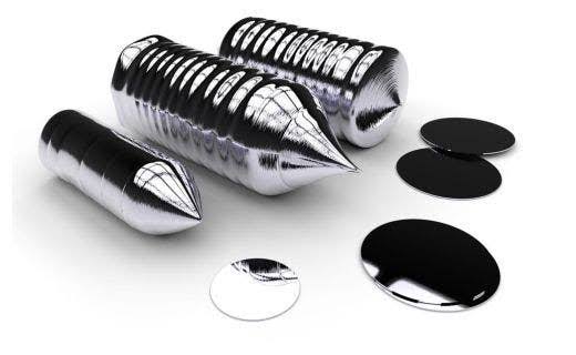
This highly ordered structure is one of the main reasons single-crystal silicon is widely used as a semiconductor material. The consistent crystal structure provides predictable electrical behavior and supports the precise control required in semiconductor manufacturing. Single-crystal silicon is commonly used to produce silicon wafers for integrated circuits, power devices, sensors and photovoltaic cells.
The crystal structure also affects how the material behaves during processing. Single-crystal silicon is anisotropic, which means that its mechanical properties can vary depending on the crystal orientation. During cutting, grinding and other machining processes, the selected cutting direction may therefore influence material removal behavior, surface quality and the risk of cracking.
Single-Crystal Silicon vs Polycrystalline Silicon
| Property | Single-Crystal Silicon | Polycrystalline Silicon |
|---|---|---|
| Crystal Structure | Continuous crystal structure | Multiple crystal grains |
| Grain Boundaries | No internal grain boundaries | Contains grain boundaries |
| Material Uniformity | Higher | More variable |
| Electrical Behavior | Highly consistent | Influenced by grain boundaries |
| Processing Behavior | Strongly affected by crystal orientation | Influenced by grain structure |
| Typical Applications | Semiconductor wafers, precision devices, high-efficiency solar cells | Solar cells and other silicon applications |
The choice between single-crystal silicon and polycrystalline silicon depends on the required electrical, mechanical and economic performance. Where high material consistency and precise semiconductor performance are required, single-crystal silicon remains the preferred silicon material.
Key Properties of Single-Crystal Silicon
Single-crystal silicon combines several important physical, mechanical and electrical properties. These properties make it highly valuable for modern electronics but also create challenges during silicon processing and cutting.
Crystal Structure and Anisotropy
Single-crystal silicon has a diamond cubic crystal structure. Its lattice structure is highly ordered, with a lattice constant of approximately 5.43 Å. The orientation of the crystal can influence its mechanical behavior, which is why crystal planes such as <100>, <110> and <111> are important in semiconductor processing.
Because of this anisotropic behavior, silicon may respond differently to cutting forces depending on the machining direction. Engineers working with single-crystal silicon therefore often consider crystal orientation when optimizing cutting, grinding or precision machining processes.
Mechanical Properties
Single-crystal silicon is relatively hard but has low fracture toughness compared with ductile engineering materials. Its elastic modulus can vary depending on crystal orientation, generally falling within a broad range of approximately 130 to 190 GPa.
The material can undergo elastic deformation under relatively small loads, but excessive localized stress may lead to brittle fracture. During machining, this behavior can result in:
- Edge chipping
- Microcracks
- Surface fractures
- Subsurface damage
These characteristics are particularly important when cutting thin silicon wafers or producing precision components.
Electrical and Thermal Properties
Silicon has a bandgap of approximately 1.12 eV at room temperature, making it suitable for a wide range of semiconductor devices. It also offers useful thermal properties, including relatively high thermal conductivity and good stability under elevated temperatures.
The melting point of silicon is approximately 1414°C. Its thermal expansion behavior must also be considered during high-temperature processing.
Why These Properties Matter During Processing
The hardness and brittle nature of single-crystal silicon are particularly important during cutting and machining. Excessive cutting forces can cause chipping, cracking and subsurface damage, while poor process control can increase material loss.
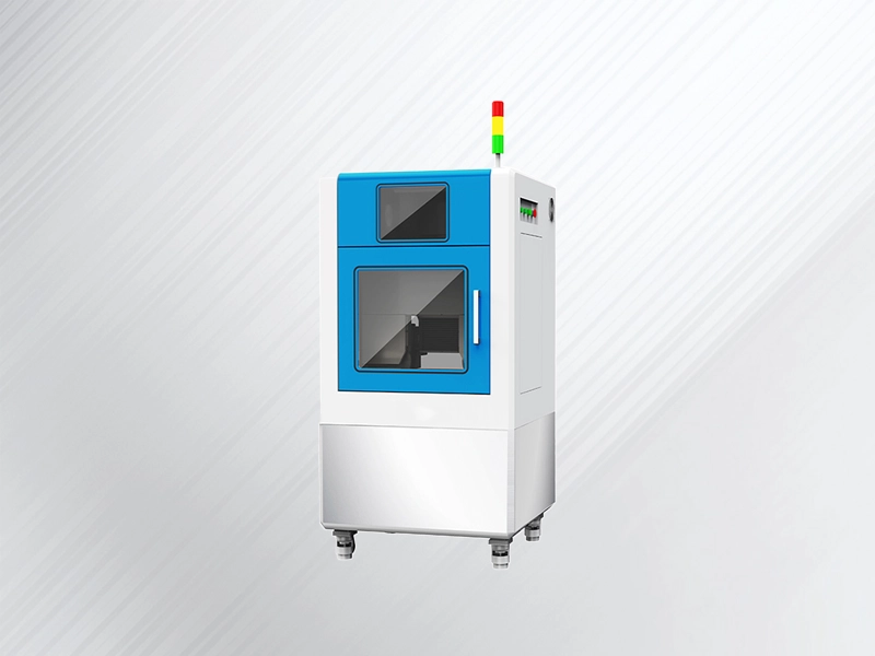
For this reason, precision cutting equipment and carefully selected abrasive tools are often required when processing silicon and other hard and brittle materials. For applications requiring controlled mechanical cutting, a diamond wire cutting machine can provide a practical solution for precision sectioning and material removal.
Why Is Single-Crystal Silicon Difficult to Process?
The processing challenges associated with single-crystal silicon are largely related to its brittle mechanical behavior and high material value.
Brittleness and Fracture
Unlike ductile metals, silicon does not normally undergo large amounts of plastic deformation before fracture. When machining forces exceed the material’s local fracture limits, cracks can form and propagate through the crystal.
This can result in:
- Surface chipping
- Edge damage
- Microcracking
- Larger fractures
The risk becomes particularly important when processing thin wafers or small precision components.
Surface and Subsurface Damage
A surface may appear smooth after cutting while microscopic damage remains beneath it. Subsurface damage can affect the mechanical strength and performance of a finished silicon wafer or component.
Depending on the cutting method and process parameters, subsequent processes such as grinding, lapping, etching and polishing may be required to remove the damaged surface layer.
Material Loss
Silicon ingot cutting and silicon wafer slicing can produce significant material loss if the cutting method creates a wide kerf. Since high-quality silicon is valuable, reducing kerf loss is an important economic objective.
This is one reason narrow cutting technologies such as diamond wire cutting have become important in modern silicon processing.
Crystal Orientation
Because single-crystal silicon is anisotropic, the crystal orientation can influence the way cracks form and propagate. The cutting direction may affect cutting forces, surface damage and material removal behavior.
These challenges make single-crystal silicon machining a specialized form of brittle material machining. The cutting method, machine rigidity, abrasive characteristics and process parameters all need to work together.
How Is Single-Crystal Silicon Produced?
Single-crystal silicon is produced through carefully controlled crystal growth processes. Before crystal growth, silicon must first be purified to the required level.
The two best-known methods for producing single-crystal silicon are the Czochralski process and the Float Zone method.
Czochralski Process
The Czochralski process, often called the CZ method, is one of the most widely used methods for producing single-crystal silicon.
High-purity polysilicon is melted in a crucible at a temperature above the melting point of silicon. A seed crystal is then brought into contact with the molten silicon. By carefully controlling rotation, temperature and pulling speed, a large silicon crystal can gradually grow from the melt.
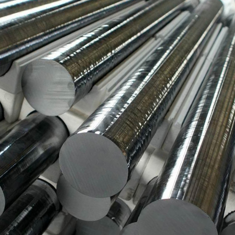
The result is a cylindrical single-crystal silicon ingot, often referred to as a silicon boule.
The CZ method is widely used because it supports large-scale production and is suitable for many semiconductor and photovoltaic applications.
Float Zone Method
The Float Zone, or FZ, method is used when very high purity and low impurity levels are required.
Unlike the CZ process, the Float Zone method does not rely on a crucible to contain the molten silicon. A localized molten zone is created and moved along a silicon rod. As the molten zone travels, impurities can be reduced and the crystal structure can be controlled.
Float Zone silicon is commonly associated with high-purity and high-resistivity applications.
CZ vs Float Zone Silicon
| Feature | Czochralski Silicon | Float Zone Silicon |
|---|---|---|
| Growth Method | Crucible-based crystal growth | Crucible-free zone melting |
| Purity | High | Very high |
| Oxygen Content | Higher | Lower |
| Production Cost | Generally lower | Generally higher |
| Typical Applications | Semiconductor and photovoltaic manufacturing | High-purity and high-resistivity applications |
Once the silicon crystal has been grown into an ingot, it must undergo a series of cutting, slicing and machining processes before it can be used in semiconductor, photovoltaic or other precision applications.
Single-Crystal Silicon Processing Flow
The processing route from a silicon ingot to a finished wafer or component can vary depending on the final application. However, a typical single-crystal silicon processing flow includes the following stages.
Step 1: Crystal Growth
A single-crystal silicon ingot is produced using a process such as the Czochralski or Float Zone method.
Step 2: Silicon Ingot Preparation
The ingot is inspected and prepared for further processing. Depending on the application, diameter control or external surface preparation may be required.
Step 3: Cropping and Sectioning
The head and tail sections of the silicon ingot may be removed, and the ingot may be sectioned into usable lengths.
Step 4: Precision Cutting or Shaping
Depending on the final application, the ingot may be shaped, squared or further sectioned. Precision cutting is important because it establishes the starting geometry for later processes.
For applications where controlled cutting forces and reduced material loss are important, diamond wire cutting machines are commonly used for precision cutting of hard and brittle materials.
Step 5: Wafer Slicing
The silicon ingot or prepared block is sliced into thin wafers. This is one of the most important stages in silicon wafer manufacturing because cutting accuracy and kerf loss directly affect material utilization.
Step 6: Surface Processing
Grinding, lapping, etching and polishing may be used to improve flatness and remove damaged surface layers.
Step 7: Precision Machining
Some silicon components require additional features such as grooves, holes, slots or complex profiles. These operations may be performed after the main cutting stage.
How Is Single-Crystal Silicon Cut?
Single-crystal silicon can be cut using several technologies, including diamond wire cutting, diamond blade sawing, wire electrical discharge machining, laser processing and precision machining.
The best method depends on factors such as:
- Material size
- Required geometry
- Required surface quality
- Production volume
- Acceptable kerf loss
- Required dimensional accuracy
For silicon ingots and many precision sectioning applications, mechanical cutting methods remain important because they can provide controlled material removal without relying on high-temperature processes.
Key Cutting Methods for Single-Crystal Silicon
| Cutting Method | Best For | Main Advantage | Main Limitation |
|---|---|---|---|
| Diamond Wire Cutting | Ingots and precision sectioning | Narrow kerf and controlled cutting | Requires suitable wire and process control |
| Diamond Blade Sawing | General sectioning | Established and widely available | Higher kerf loss |
| WEDM | Conductive precision components | Can produce complex shapes | Limited to conductive materials and slower processing |
| Laser Processing | Fine features and localized cutting | Non-contact processing | Possible thermal effects |
| CNC Machining | Complex shapes and features | High flexibility | Often used as a secondary process |
Diamond Blade Sawing
Diamond blade sawing remains useful for certain sectioning applications. However, the wider cutting kerf can increase material loss, which is an important consideration when processing high-value silicon.
Wire Electrical Discharge Machining
WEDM removes material through controlled electrical discharges. It can be useful for conductive materials and complex geometries, but the process may create a recast layer or surface effects that require further processing.
Laser Processing
Laser processing offers non-contact material removal and can be useful for localized operations. However, thermal effects must be carefully controlled when surface integrity is important.
CNC Machining
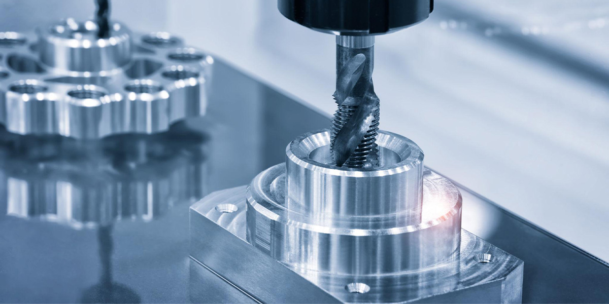
CNC machining can be used to produce slots, holes and complex features. In many applications, it is used after primary cutting rather than as the main method for slicing large silicon ingots.
Diamond Wire Cutting for Single-Crystal Silicon
Diamond wire cutting is one of the most important technologies for processing hard and brittle materials such as single-crystal silicon.
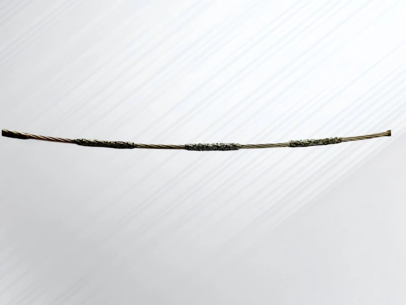
The process uses a wire carrying diamond abrasives to remove material through controlled mechanical grinding. As the wire moves through the workpiece, the diamond particles gradually remove silicon from the cutting zone.
One of the main advantages of diamond wire cutting is the potential to reduce kerf loss compared with wider cutting tools. A narrower cutting path means that more of the original silicon material can remain available for finished products.
Diamond wire cutting can also provide several other advantages:
- Controlled cutting forces
- Reduced material loss
- Good cutting accuracy
- Suitability for hard and brittle materials
- Flexible cutting of different workpiece sizes
However, cutting performance depends heavily on the complete process. Wire characteristics, tension, cutting speed, feed rate and machine stability all influence the final result.
For manufacturers processing silicon ingots, crystals and other brittle materials, selecting a suitable diamond wire cutting machine is therefore only one part of the solution. The wire and process parameters must also match the material and cutting requirements.
The Role of Diamond Wire in Silicon Cutting
The cutting wire itself is a critical part of the diamond wire cutting process.
Wire Diameter
Wire diameter influences both cutting stability and kerf width. A thinner wire can reduce the amount of material removed during cutting, while a larger wire may offer different mechanical characteristics depending on the application.
The correct diameter should therefore be selected according to the material size, cutting stability and required surface quality.
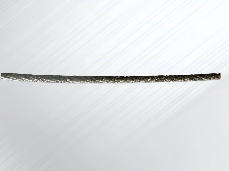
Diamond Coating
The diamond abrasive determines the cutting action. Abrasive size, density and bonding characteristics can influence cutting efficiency, wire wear and surface finish.
Wire Tension
Proper tension helps maintain cutting stability. Insufficient tension can reduce cutting accuracy, while excessive tension can increase the risk of wire failure.
Cutting Speed
Higher speed does not automatically produce better results. Cutting speed must be balanced with feed rate, abrasive performance and machine stability.
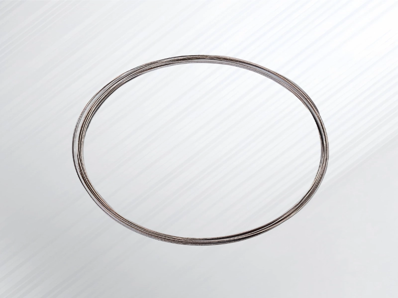
For applications requiring a closed-loop cutting tool, selecting a suitable diamond wire loop can be an important part of optimizing the cutting process.
The best diamond wire selection depends on the specific application rather than a single universal specification.
Precision Machining After Silicon Cutting
Primary cutting does not always produce the final shape required by the end user. Many silicon components require additional precision machining.
Typical secondary operations may include:
- Grooves
- Slots
- Holes
- Edge features
- Complex profiles
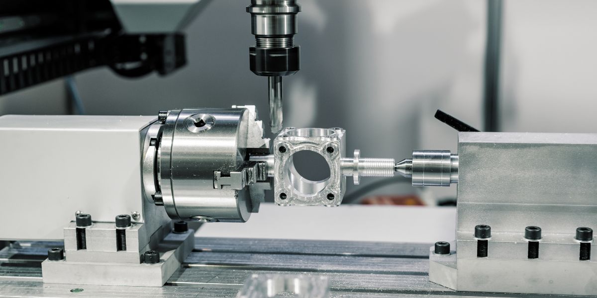
For these applications, CNC-based engraving and milling systems can provide greater flexibility for shaping and feature generation.
A suitable engraving and milling machine can be used for precision machining tasks where controlled tool movement and complex geometry are required.
This creates a practical processing chain:
Primary Cutting → Precision Slicing → Secondary Machining
Each stage has different requirements for cutting forces, tooling and dimensional control.
Understanding the Brittle-to-Ductile Transition in Silicon Processing
Single-crystal silicon is generally considered a brittle material. However, under carefully controlled conditions, localized material removal may shift toward a more ductile mode.
This behavior is often described as the brittle-to-ductile transition.
At very small material removal scales, controlled machining conditions may reduce the formation of large cracks and improve surface quality. The transition depends on several factors, including:
- Cutting depth
- Abrasive size
- Cutting speed
- Feed rate
- Tool geometry
- Machine rigidity
For precision silicon machining, the goal is often to control material removal so that unnecessary fracture and deep cracking are minimized.
This is particularly important when manufacturing thin wafers and precision silicon components where surface integrity is critical.
How to Choose the Right Single-Crystal Silicon Processing Method
The best processing method depends on the required product.
For Silicon Ingot Sectioning
Diamond wire cutting can be a suitable option when controlled cutting and reduced material loss are important.
For Wafer Preparation
Precision wire slicing is commonly used when producing thin silicon wafers with controlled thickness and efficient material utilization.
For Complex Shapes
CNC machining may be more suitable for components requiring slots, holes or complex profiles.
For Fine Features
WEDM or laser processing may be considered depending on material properties and feature requirements.
For Secondary Machining
Engraving and milling can provide flexibility for additional shaping after the main cutting process.
The best approach is to evaluate the complete process rather than selecting equipment based on cutting speed alone.
Applications of Single-Crystal Silicon
Single-crystal silicon is used in many industries because of its electrical, thermal and mechanical properties.
Semiconductor Manufacturing
Single-crystal silicon is the foundation of most semiconductor wafer production. Silicon wafers are used as substrates for integrated circuits, processors, memory devices and many other electronic components.
Photovoltaic Manufacturing
Monocrystalline silicon is widely used in high-efficiency solar cells. Continued development in photovoltaic manufacturing has increased the importance of material utilization and precision wafer slicing.
For cutting processes related to photovoltaic materials, specialized solar cell material cutting solutions can help address the requirements of silicon and other brittle materials.
MEMS and Sensors
Silicon is widely used in MEMS devices, accelerometers, pressure sensors and other precision components.
Optical and Scientific Applications
Silicon may also be used in specialized optical, scientific and research applications where its material properties and crystal structure provide useful performance.
Frequently Asked Questions About Single-Crystal Silicon
What is single-crystal silicon?
Single-crystal silicon is silicon with a continuous and highly ordered crystal structure. It is widely used in semiconductor wafers, solar cells and precision electronic components.
What is the difference between single-crystal and polycrystalline silicon?
Single-crystal silicon has a continuous crystal structure with no internal grain boundaries, while polycrystalline silicon consists of multiple crystal grains.
How is single-crystal silicon produced?
It is commonly produced using the Czochralski process or the Float Zone method.
How is single-crystal silicon cut?
Single-crystal silicon can be processed using diamond wire cutting, diamond blade sawing, WEDM, laser processing and precision machining. The best method depends on the required geometry and production requirements.
Why is diamond wire used to cut silicon?
Diamond is extremely hard and can remove silicon through controlled abrasive cutting. Diamond wire cutting can also help reduce kerf loss and control cutting forces.
What is the best method for cutting a silicon ingot?
The best method depends on the ingot size, required geometry and material utilization requirements. Diamond wire cutting is widely used for precision sectioning and silicon processing because of its narrow cutting path and suitability for brittle materials.
Can single-crystal silicon be machined with CNC equipment?
Yes. CNC equipment can be used for secondary machining operations such as producing grooves, holes, slots and complex profiles.
What causes chipping during silicon cutting?
Chipping can result from excessive cutting forces, unstable machining conditions, unsuitable tools or process parameters. The brittle nature of silicon also makes crack formation more likely.
Conclusion
Single-crystal silicon is a high-value material whose unique properties require careful processing. Its crystal structure, semiconductor performance and material consistency make it essential for semiconductor, photovoltaic and precision engineering applications, but its hardness and brittleness also create significant machining challenges.
Different stages of processing may require different technologies, including ingot sectioning, wafer slicing and secondary precision machining. Reducing material loss, controlling surface damage and maintaining stable cutting conditions are all important for improving process efficiency and finished product quality.
For applications involving hard and brittle materials, explore Zelatec’s product range, including diamond wire cutting machines, diamond wire loops and engraving and milling machines, to find equipment suitable for different cutting and precision machining requirements.