Facing SiC Cutting Challenges: Have You Encountered These?
Silicon carbide (SiC) is a synthetic compound of silicon and carbon, formed at high temperatures. With a Mohs hardness of 9.5, it is second only to diamond, but also highly brittle—more like a ceramic than a metal.
Despite existing in many crystal forms (polytypes), its extreme hardness, chemical stability, high thermal conductivity, and wide electronic bandgap remain consistent. These fixed traits define the physical profile any cutting process must work within.
In actual mass production, the gap between “getting a cut done” and “achieving high-yield precision” is where most processes fail. Many manufacturers find themselves struggling with the same recurring issues:
Is chipping depth still exceeding tolerances during ingot cropping or slicing?
Is wire vibration leaving micro-cracks that compromise the wafer’s integrity for downstream epi-growth?
Is the width of the cut wasting far too much of your expensive, slow-grown SiC material?
Is your cutting speed bottlenecking output just as downstream demand surges? Does pushing for higher speed always force a sacrifice in surface quality?
Can your process reliably hold TTV (Total Thickness Variation), bow, and warp to epi-grade tolerances at scale?
Are uneven wire wear and unexpected breaks inflating your per-wafer cost and causing unplanned downtime?
Do larger-diameter wafers (6-inch to 8-inch transitions) expose hidden instabilities in your current equipment setup?
Our Solution: A Stabilized Ecosystem for High-Yield SiC Processing
At Zelatec, we don’t view Silicon Carbide as just another material to cut—we treat it as a high-value asset that requires a stabilized, science-based approach. Our integrated solution combines advanced diamond wire technology with precision mechanical platforms to solve the paradox of SiC: achieving high throughput without compromising crystal integrity.
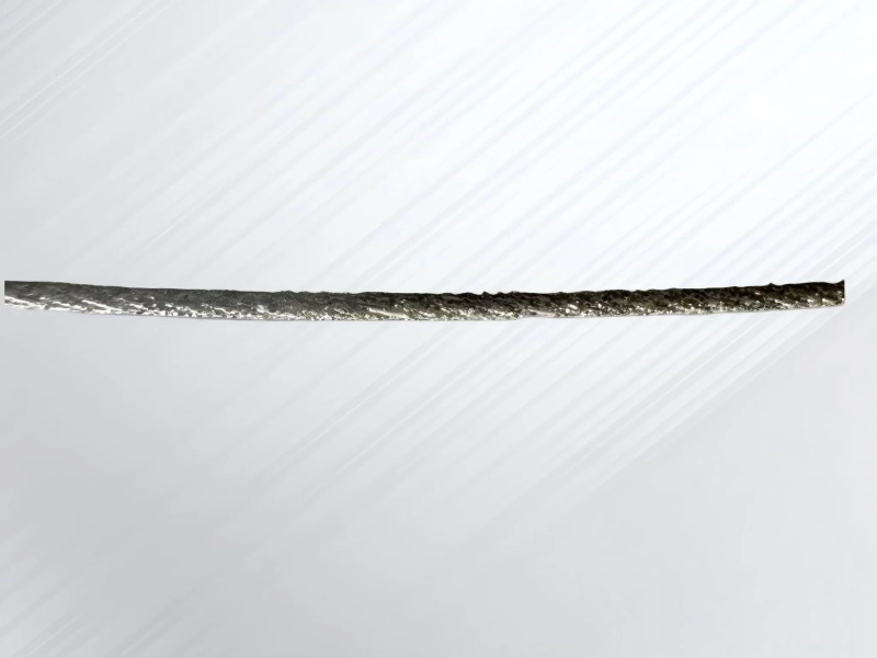
The most direct way to increase your ROI is to reduce material waste. Our specialized diamond wires are engineered for the extreme hardness of SiC while maintaining a minimal diameter.
-
Maximizing Ingot Utilization: By minimizing the “kerf” (the width of the cut), our thin-wire technology allows you to extract more wafers from every single ingot.
-
Optimized Grit Retention: Using a proprietary electroplating process, we ensure diamond particles stay bonded to the wire even under high-load cutting, preventing “bald spots” that cause uneven surfaces.
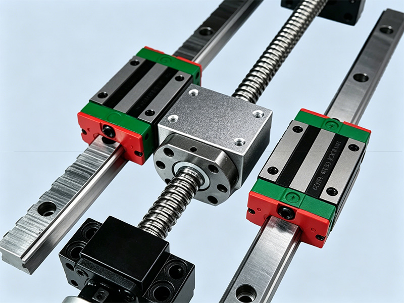
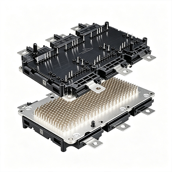
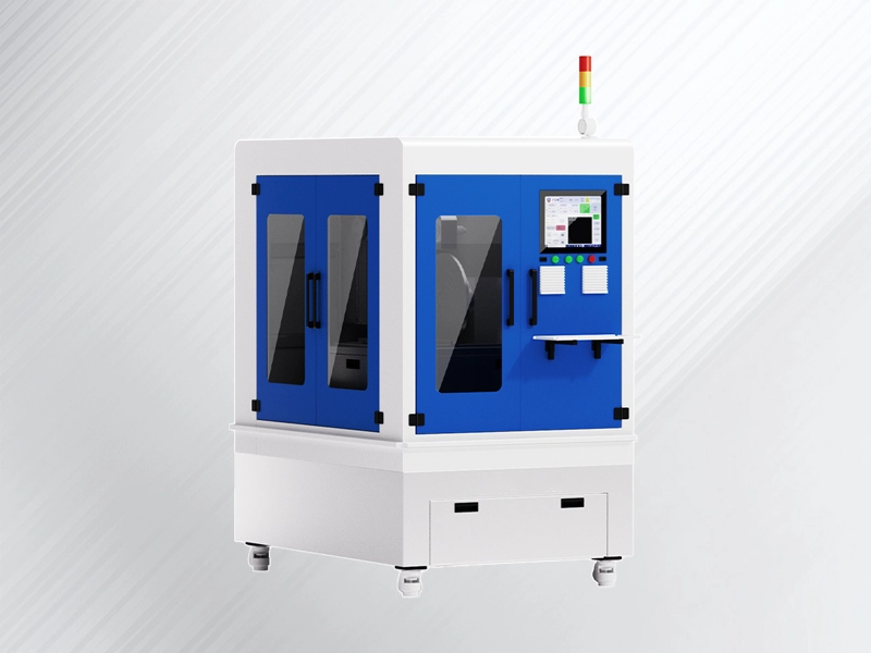
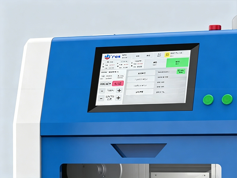
A high-quality wire is only as good as the machine driving it. Zelatec cutting machines are built for the mechanical rigidity required to handle 9.5 Mohs hardness materials.
-
Active Tension Management: Our systems feature a high-response closed-loop tension control. This eliminates “wire-bowing” and vibration, the primary culprits behind Sub-Surface Damage (SSD) and micro-cracks.
-
Geometric Accuracy: We reliably hold TTV (Total Thickness Variation), Bow, and Warp to within epi-grade tolerances, significantly reducing the time and cost of downstream double-side grinding and polishing.
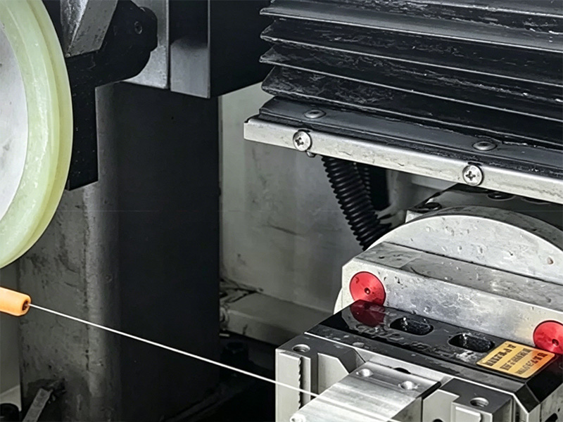
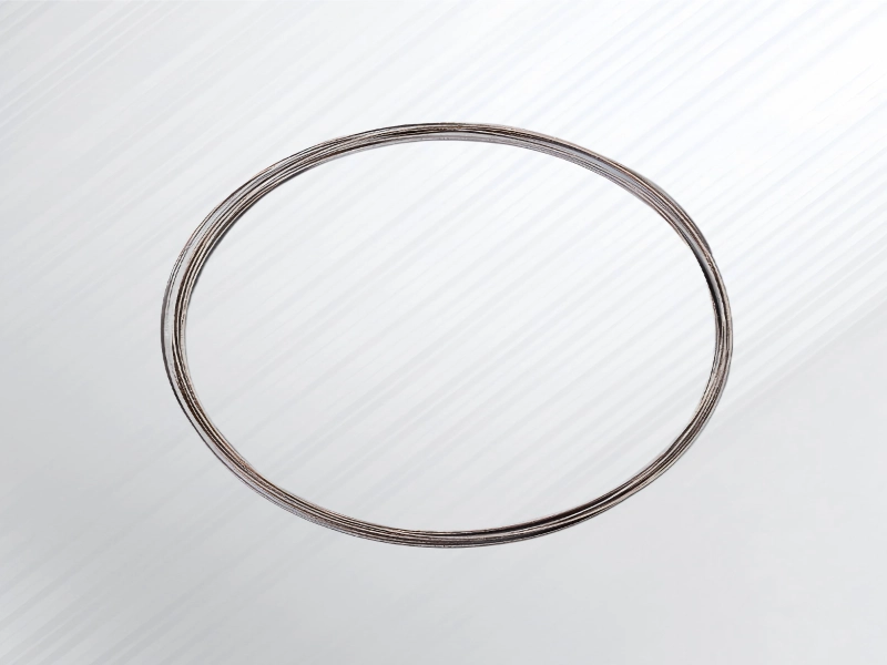
For manufacturers facing a surge in demand, our Diamond Wire Loop technology represents the cutting edge of throughput efficiency.
-
Constant High-Speed Removal: Unlike reciprocating saws that must decelerate to change direction, our endless loop maintains a constant linear speed (up to 60 m/s). This results in a 3x to 5x increase in cutting efficiency compared to traditional methods.
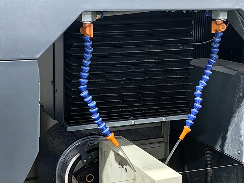
SiC cutting generates intense heat and abrasive swarf. Our solution maintains a stabilized environment to protect wafer integrity.
-
Rapid Cooling: Closed-loop systems maintain constant temperatures, preventing thermal cracking and the “potato-chip” warping effect.
-
Advanced Filtration: Continuous swarf removal prevents “double cutting” and surface scoring, ensuring a consistently low Ra (Surface Roughness).
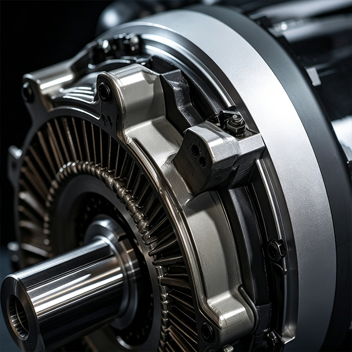
Zelatec covers the entire pre-wafering workflow, ensuring consistency from the raw boule to the final slice.
-
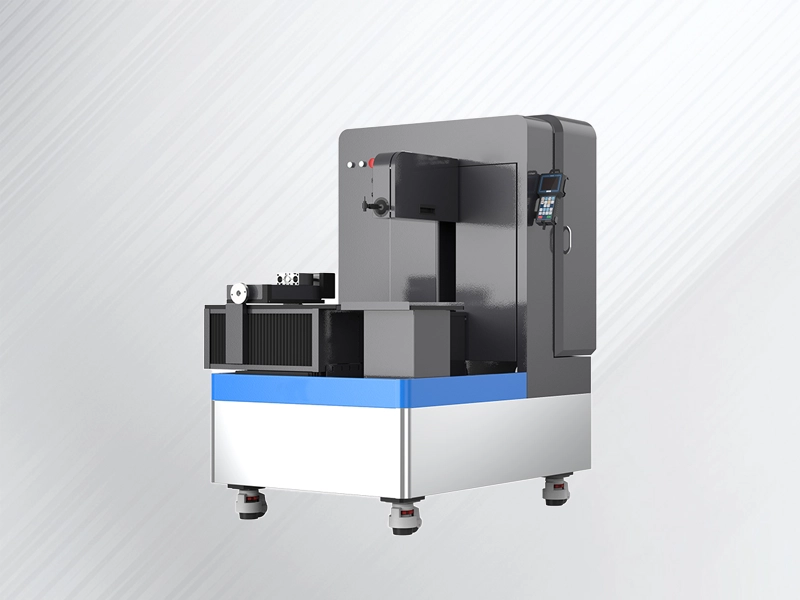
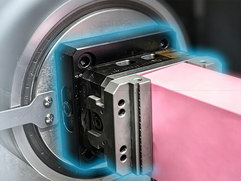
Ingot Cropping: Heavy-duty, high-torque platforms remove seeds and tails with zero vibration, even under high-load demands.
-
Precision Squaring: Specialized fixtures square cylindrical boules into high-precision blocks while preserving critical crystal orientation.
-
Adaptive Scaling: Modular clamping systems offer the rigidity needed for everything from 2-inch R&D crystals to 8-inch mass production ingots.
We provide more than just hardware; we provide the “recipe” for stable production. Our technical team supports you in fine-tuning the balance between wire speed, feed rate, and tension based on your specific material (4H-SiC, 6H-SiC, or Polycrystalline).
-
Predictable Consumable Life: Our data-driven approach helps you forecast wire wear, preventing unplanned downtime and protecting your boules from mid-cut wire breaks.
Production Workflow
Crystal Growth
SiC boule produced via physical vapor transport (PVT).
Ingot Grinding
Diameter precision and crystal plane alignment set for slicing.
Cropping
Ingot ends removed; edge chipping control is critical at this stage.
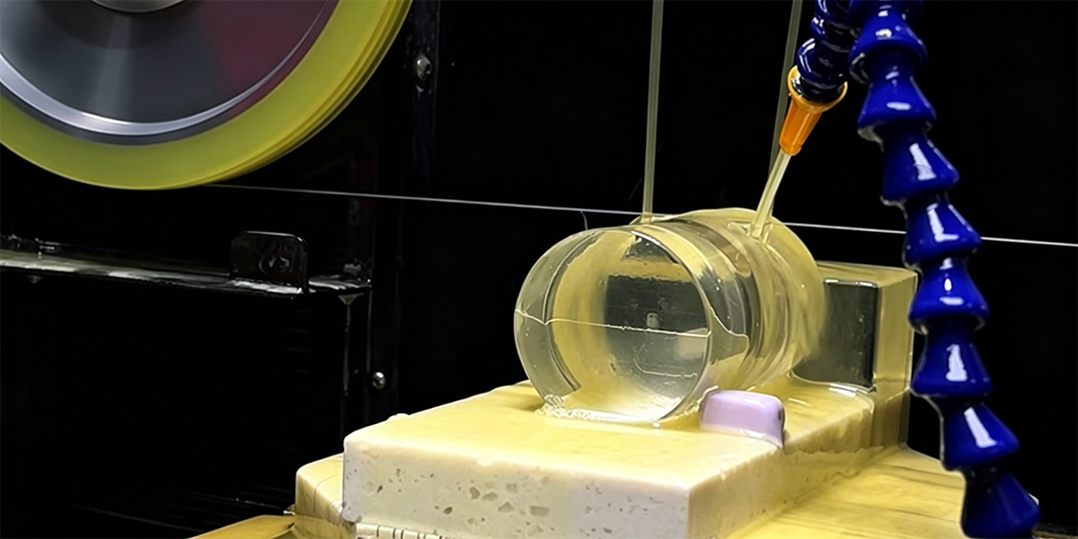
Multi-wire Slicing
Wafers sliced from ingot; TTV, bow, warp, SSD, and kerf width established here.
Edge Rounding
Edge profiling to eliminate micro-cracks and reduce breakage risk.
Grinding / Lapping
Removes subsurface damage and saw marks, improves flatness.
CMP Polishing
Atomically flat, damage-free surface for epitaxial growth.
Final QC
Cleaning, inspection under high-intensity light, and packaging.
Is Diamond Wire Sawing the Most Common SiC Cutting Tool? How It Compares
Fixed-abrasive diamond wire sawing is today’s standard for slicing SiC ingots — it balances throughput, narrow kerf, and manageable surface damage. The table below shows how it stacks up against the other cutting approaches found in SiC manufacturing.
| Cutting Method | How It Works | Strengths for SiC | Limitations | Typical Use |
| Fixed-Abrasive Diamond Wire Sawing | Diamond grit bonded to a wire; the wire grinds through the crystal. | High productivity, narrower kerf → more wafers per ingot, lower damage, proven on 150–200 mm ingots. | Wire wear & breakage need monitoring; recipe tuning required. | Mainstream ingot slicing and cropping. |
| Mortar (Loose-Abrasive) Sawing | Bare wire runs through abrasive slurry; the slurry does the cutting. | Established, can process multiple wafers. | Slower, messy slurry handling, wider kerf, wire wear. | Legacy lines being replaced. |
| Laser Cutting (Ablation/Stealth) | Laser melts material or creates a weak layer for separation. | Very high potential speed, narrow cut, no tool wear. | Thermal damage or extra separation step; high cost; still maturing for bulk slicing. | Thin wafers, niche applications. |
| Mechanical Blade Sawing | Rotating diamond blade scribes/cuts the wafer. | Simple, low equipment cost. | Rapid tool wear on SiC, severe edge chipping, poor material yield. | Small-scale or obsolete uses. |
Which Diamond Wire Is Right for Silicon Carbide (SiC) Cutting?
Three fixed-abrasive diamond wire types earn a real place in SiC cutting. The table below lays out their honest, side-by-side numbers so you can match the technology to your actual priorities — volume, material yield, or surface quality.
| Wire Technology | Bond & Motion | Typical Speed | Kerf Width | As-Cut Surface | Throughput | Best Fit |
| Electroplated (Multi-wire) | Nickel-bonded, reciprocating | 8–15 m/s | >200 µm | Good but carries reversal marks, waviness, and edge chipping | Very high (hundreds of wafers simultaneously) | High-volume production with established post-processing |
| Resin Bonded | Polymer matrix, reciprocating | Lower | Variable, widens with wear | Can be gentle initially, quickly becomes inconsistent | Negligible for production-scale SiC | Rare lab trials or non-critical dicing; not for industrial SiC |
| Diamond Wire Loop | Nickel-bonded closed loop, unidirectional | 40–80 m/s | ≤0.3 mm | Very uniform, minimal chipping, no reversal marks | Small-batch, precision-focused (single wire) | High-value R&D, thin wafers, maximizing wafers per ingot |