Industry Insights
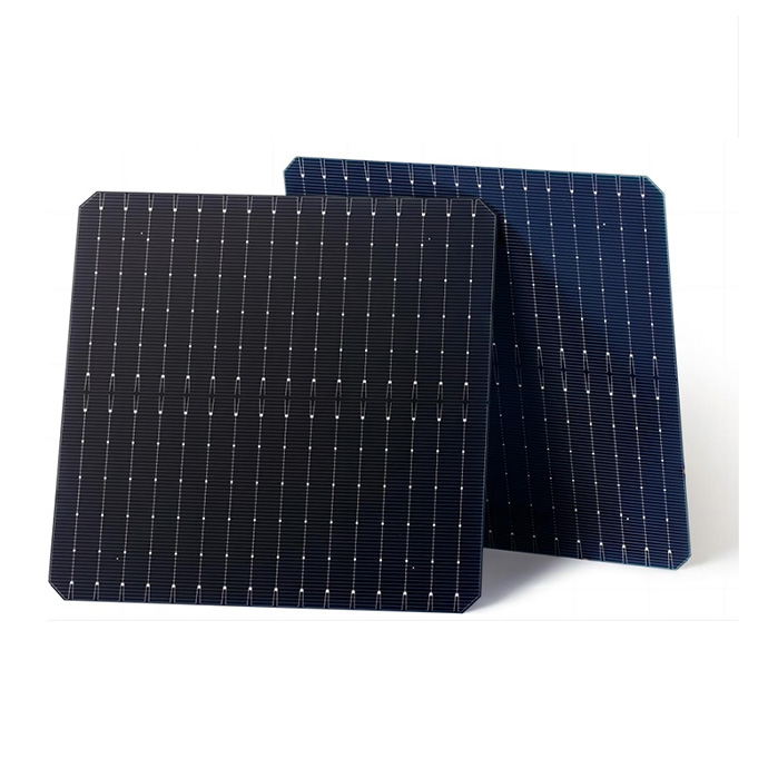
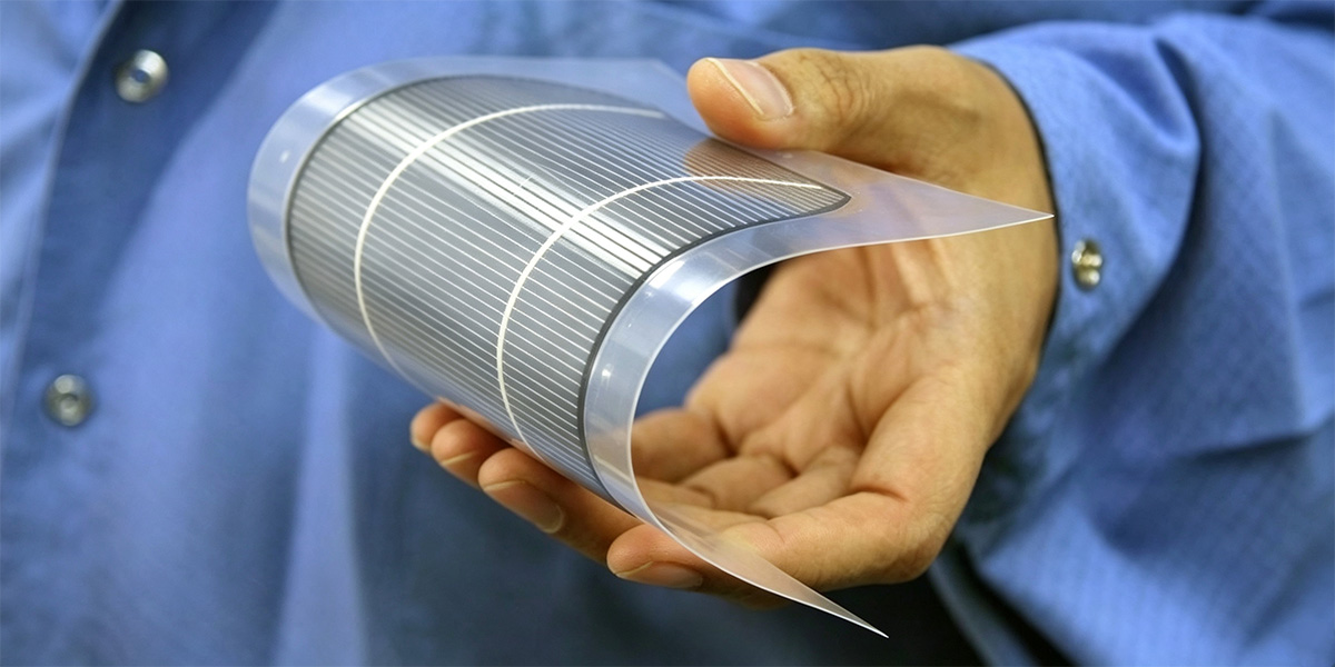
The PV industry is racing toward grid parity through relentless cost reduction. At wafer level, this means thinner wafers (n-type down to 120–130 μm), larger formats (G12 dominating), and finer diamond wires (now 28 μm) with faster cutting speeds.
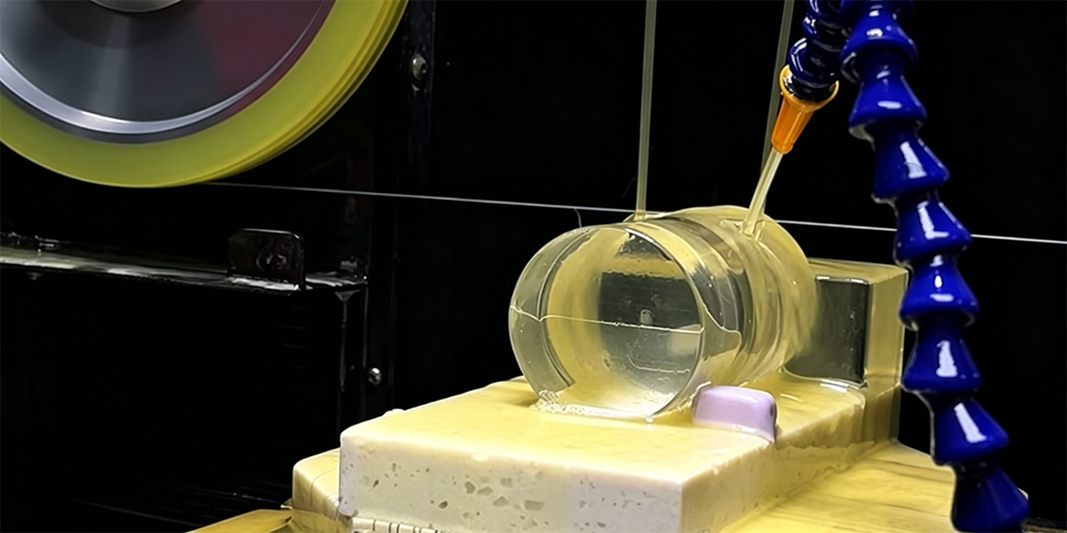
Cutting is the critical step—it determines downstream yield and cost. Silicon is hard and brittle; diamond wire sawing inevitably creates subsurface damage (SSD) 1–30 μm deep, the primary cause of wafer breakage. At 0.15 mm thickness, breakage can reach ~6%. Key challenges include wafer breakage, saw marks, warp, and wire wear—especially as wires drop below 35 μm.
The industry has shifted from slurry to diamond wire sawing (DWS), now capturing over 90% of the global PV market. DWS delivers superior surface quality, lower kerf loss, and higher efficiency. In monocrystalline slicing, DWS is near‑universal.
Mastering precision cutting directly impacts material utilization, yield, and profitability. The transition to thinner, larger wafers with finer wires is happening now—and those who optimize cutting today will lead the next phase of PV cost reduction.
Our Technical Solutions: Comprehensive Slicing Engineering for Solar Silicon
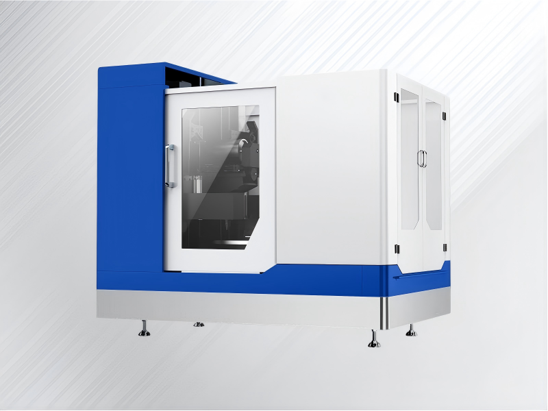
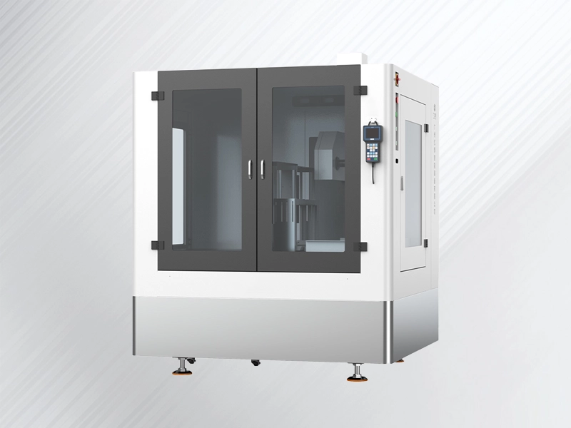
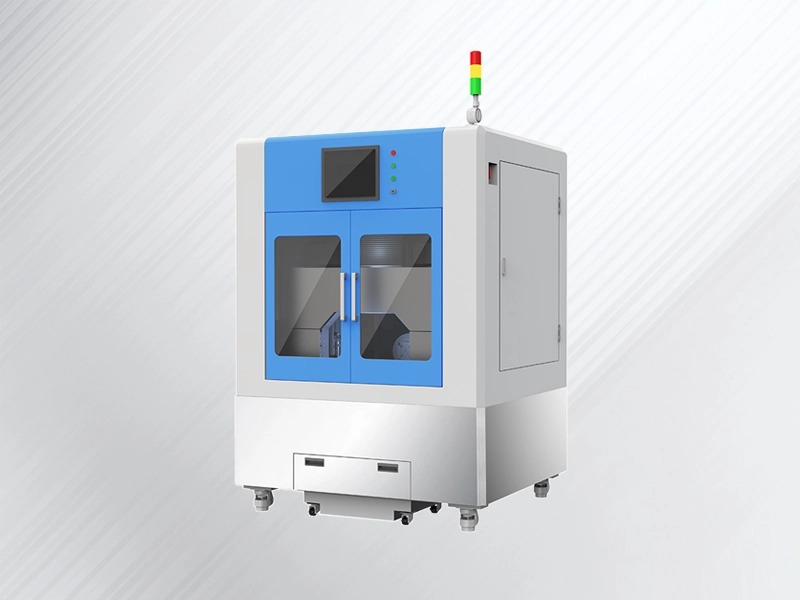
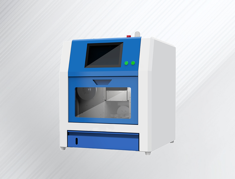
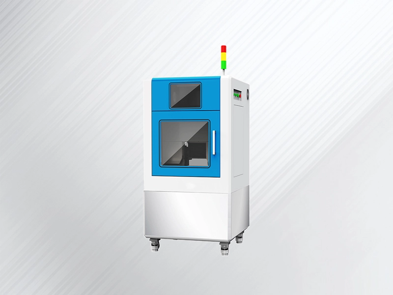
To support the industry-wide transition toward thinner N-type TOPCon and HJT substrates, our diamond wire and slicing equipment solutions address three critical physical priorities: minimizing kerf loss, restricting geometric tolerances (TTV/Warp), and suppressing wire breakage under continuous high-speed tension.
We deliver specialized diamond wire consumables, precision equipment configurations, and process parameter alignment across the three essential stages of solar silicon processing:
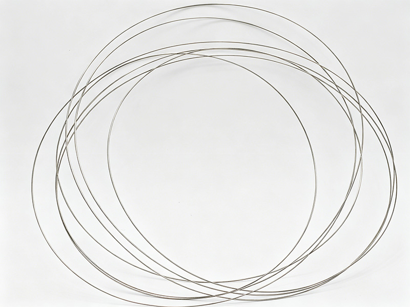
-
Application: Removing non-conforming head/tail sections and sectioning long single-crystal silicon rods into targeted brick lengths.
-
Technical Execution: Utilizes high-durability diamond wire gauges (0.18-0.25mm) with high diamond retention strength, engineered to handle large-diameter cross-sections without blade-line deflection or thermal stress cracking.
-
Primary Benefit: Delivers clean, perpendicular cut surfaces that prevent thermal micro-cracking at ingot ends, maximizing usable silicon volume prior to squaring.
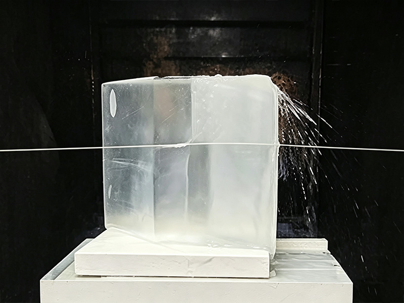
-
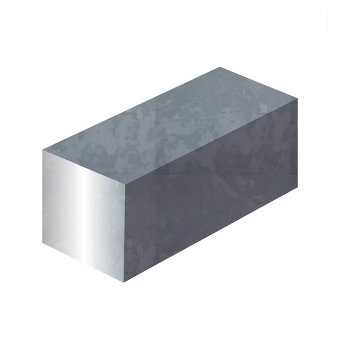
Application: Converting round silicon ingots into precise 182 mm and 210 mm square or pseudo-square bricks.
-
Technical Execution: Deploys specialized 4-wire or multi-wire squaring setups utilizing high-tensile core steel wire (>3800 MPa) with uniform grit distribution.
-
Primary Benefit: Maintains tight diagonal tolerances and straight block edges, significantly reducing edge chipping and corner micro-fractures during heavy sectioning.
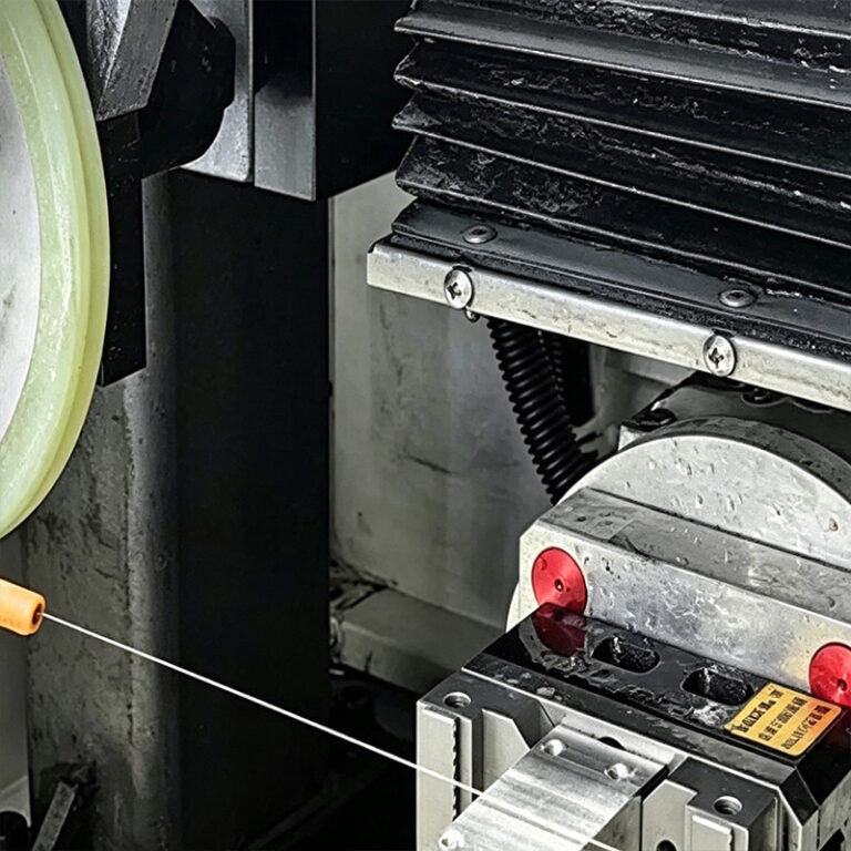
-
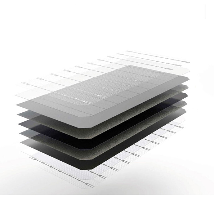
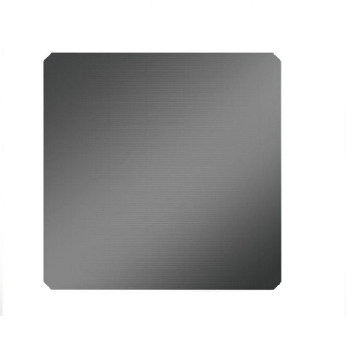
Application: High-density, multi-line slicing of square silicon bricks into ultra-thin wafers (110–130 μm) for high-efficiency cell lines.
-
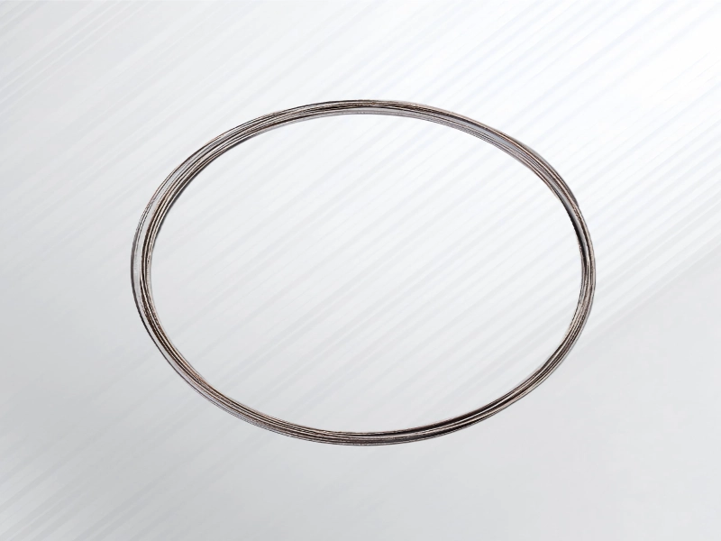
Micro-Gauge Wire Selection: Formulated with ultra-fine high-carbon steel wire (0.035–0.050 mm) to narrow kerf width, directly increasing wafer output per ingot.
-
Controlled Grit Topology: Precision-electroplated synthetic diamond grits ensure uniform multi-point micro-scraping, restricting Total Thickness Variation (TTV) to ≤ 10 μm and minimizing sub-surface damage (SSD).
-
High-Speed Operational Stability: Engineered for stable running at linear wire speeds (Vs) of 60–85 m/s with active dynamic tension control (≤ ±0.3 N fluctuation).
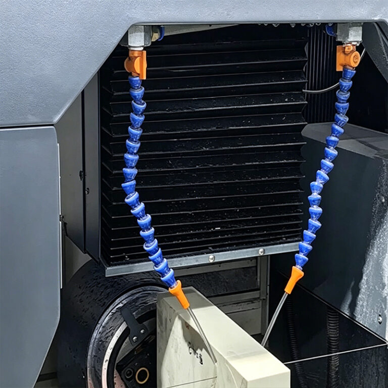
Achieving consistent wafer yield requires syncing consumable wire properties with the host machine environment. Our engineering support includes:
-
Swarf Clearance & Coolant Alignment: Optimizing wire plating density and grit clearance channels to work seamlessly with low-viscosity, water-soluble coolants—preventing diamond glazing and thermal buildup inside micro-kerfs.
-
Tension & Feed Calibration: Providing tested operational tension curves (N) and progressive feed rate (Vf) guidelines compatible with standard single-wire and multi-wire slicing equipment.
Diamond Wire Saw Application in Solar Cell Processing
Complete Ingot-to-Cell Manufacturing Chain & Key Slicing Junctions
Ingot Production
High-purity monocrystalline silicon rod growth (CZ method) or multicrystalline casting.
Ingot Cropping
Sectioning long ingots into manageable lengths while cropping off non-conforming ends.
Ingot Squaring
Shaping round ingots into standard square or pseudo-square bricks with exact dimensions.
Wafer Slicing
High-speed multi-wire web slicing bricks into thousands of ultra-thin wafers in a single pass.
Etching & Texturing
Removing subsurface damage (SSD) and texturing wafer surfaces for solar cell lines.
Cell Fabrication
Diffusion, passivation, coating, and metallization to produce active PV solar cells.
What This Means for Your Business
At the end of the day, the goal isn’t better cutting—it’s better business. Here’s how our precision cutting solutions translate into measurable value for your PV manufacturing operation.
Recommended Processing Parameter Matrix
Standard engineering baseline parameters for monocrystalline silicon processing across cropping, squaring, and multi-wire wafering stages.
| Processing Stage | Core Wire Gauge | Linear Wire Speed | Operational Tension | Feed Rate | Target Quality |
|---|---|---|---|---|---|
| Ingot Cropping | 0.18 – 0.25 mm | 30 – 50 m/s | 25 – 35 N | 1.0 – 3.0 mm/min | Clean cut, zero cracking |
| Ingot Squaring | 0.12 – 0.16 mm | 40 – 60 m/s | 18 – 25 N | 0.8 – 2.0 mm/min | Minimal edge chipping |
| Wafering (182 mm) | 0.038 – 0.045 mm | 60 – 80 m/s | 7.5 – 9.5 N | 1.2 – 2.2 mm/min | TTV ≤ 10 μm, Kerf < 55 μm |
| Wafering (210 mm) | 0.040 – 0.050 mm | 65 – 85 m/s | 8.0 – 10.5 N | 1.0 – 2.0 mm/min | TTV ≤ 10 μm, SSD < 8 μm |
* Baseline parameters for TOPCon/HJT N-type substrates. Fine-tune parameters based on machine frame rigidity and coolant pressure.