Understanding Crystal Slicing: The Real Challenges
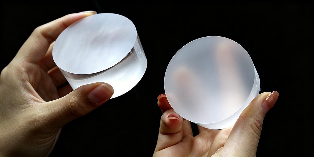
Crystals like silicon, sapphire, SiC, and YAG are essential in semiconductors and optics. But extreme hardness, low fracture toughness, and thermal sensitivity make them notoriously difficult to cut.
Edge chipping causes immediate rejection of high-value parts. Subsurface micro-cracks stay invisible until later processing—by then, parts have already incurred significant cost. Wide kerf loss turns expensive material into waste, with over 40% material loss common. Warpage and breakage worsen as wafers get thinner. Surface damage degrades device performance and optical clarity. And slow processing creates throughput bottlenecks.
Traditional cutting methods often create more problems than they solve. The real question: how do you cut crystals cleanly—without creating damage that has to be fixed later?
Our Precision Slicing Solution
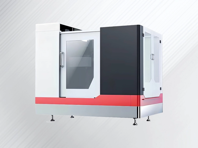
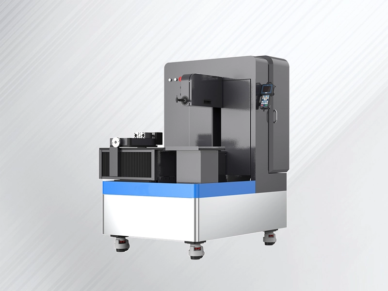
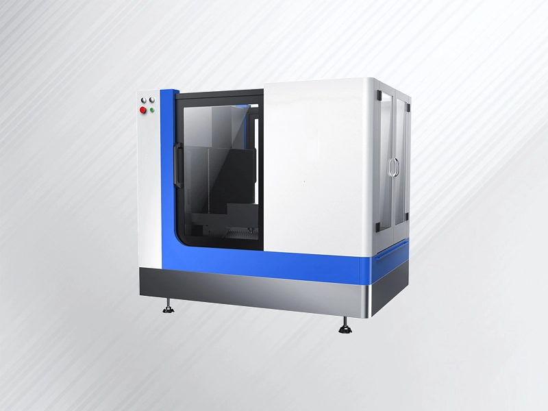
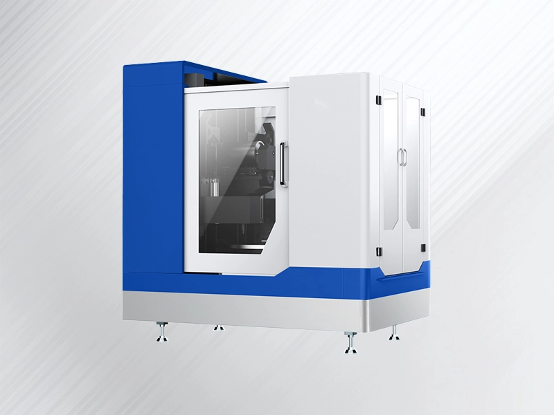
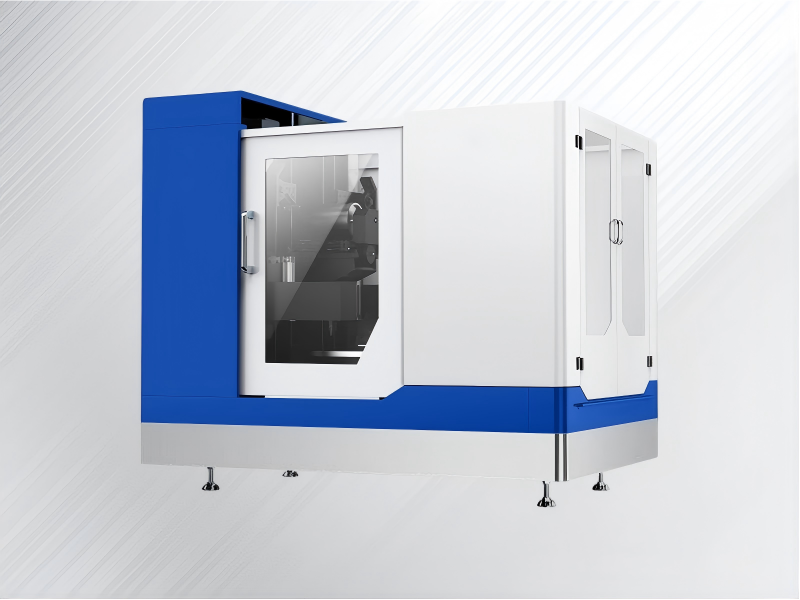
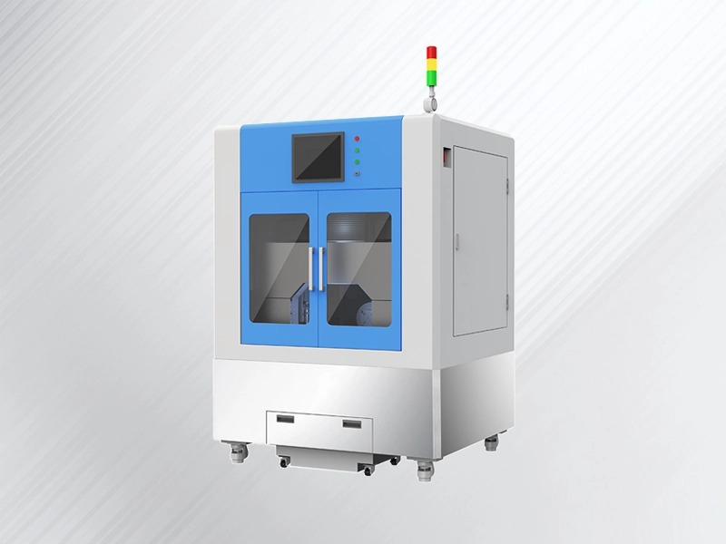
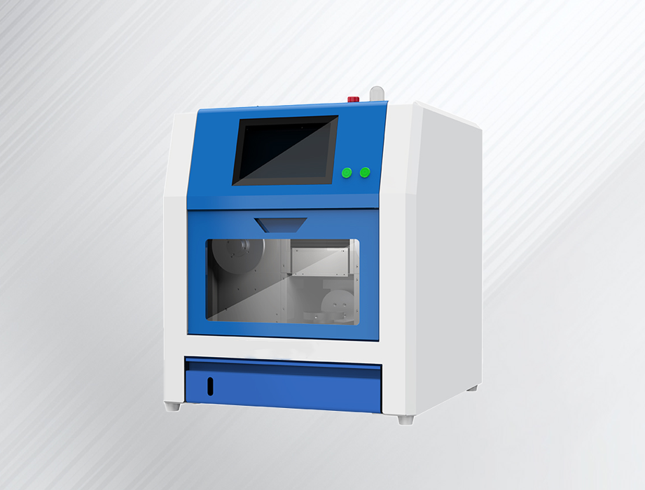
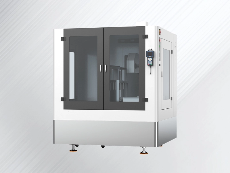
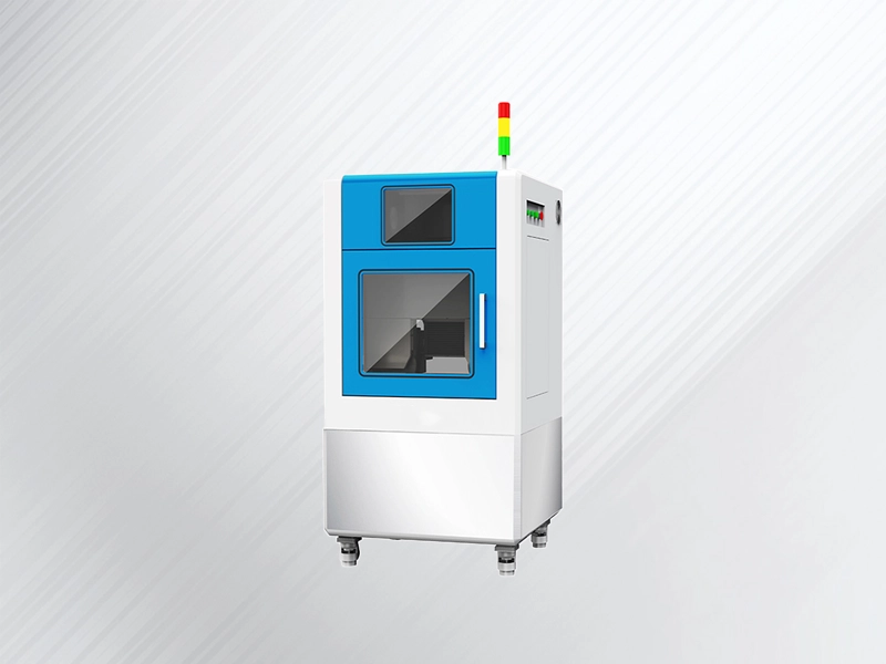
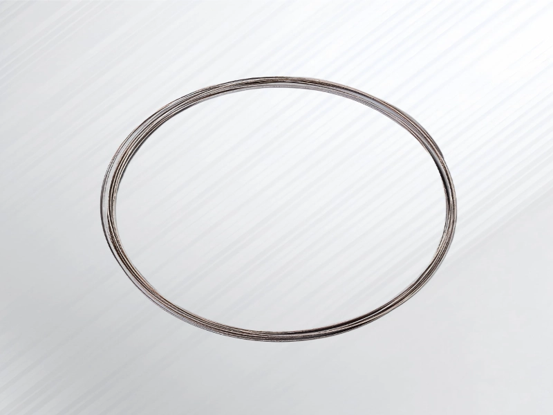
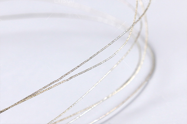
Our diamond wire slicing solution replaces traditional, aggressive rigid blades and messy slurry saws with a continuous, low-stress cutting process engineered specifically for crystal materials. By combining high-speed diamond wire motion with closed-loop tension control and continuous coolant delivery, our system solves the fundamental trade-off in crystal processing: achieving thin, fast cuts without compromising lattice integrity or surface quality.
Here is how our technology directly solves your daily production bottlenecks:
Complete Crystal Cutting Workflow
From raw grown ingot to defect-free wafers, explore how precision diamond wire sawing fits into your crystal processing pipeline to reduce kerf loss and eliminate subsurface damage.
Crystal Growth & Inspection
Single-crystal ingots are synthesized and inspected for internal stress, lattice orientation, and purity.
Squaring & Rounding
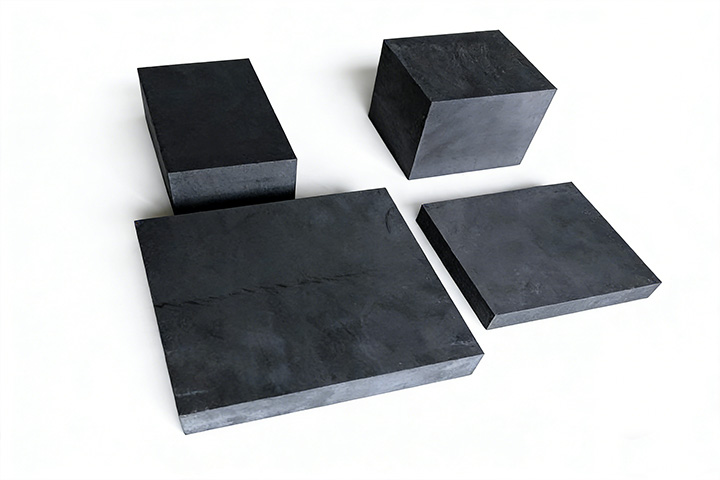
Ingots are ground to precise outer diameters or squared into blocks to establish baseline geometry.
Ingot Cropping & Sectioning
Low-stress sectioning removes seed/tail ends and cuts long ingots into blocks without thermal fractures.
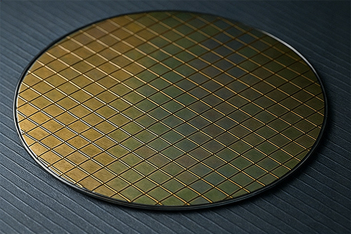
Precision Wafer Slicing
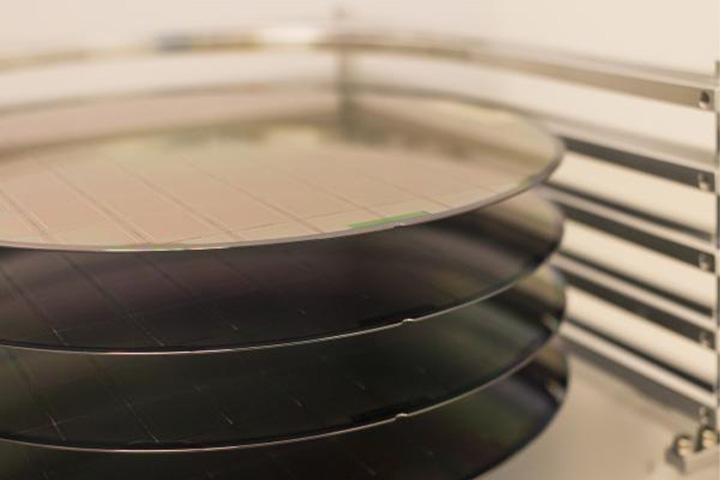
High-speed wire motion converts crystal blocks into thin wafers with narrow kerf loss (0.20–0.35 mm) and low TTV.
Edge Profiling & Lapping
Wafers are chamfered to prevent chipping. Superior cut finish allows bypassing or shortening coarse lapping.
CMP & Final Quality Assurance
Chemical-mechanical polishing produces mirror surfaces, followed by TTV, bow, warp, and surface defect checks.
Diamond Wire Saw vs. Alternative Cutting Methods
| Criteria | Diamond Wire Saw (Multi-wire) |
Diamond Wire Saw (Single-wire) |
Laser Cutting | Waterjet Cutting | ID Saw (Internal Diameter) |
Slurry Wire Saw (Free Abrasive) |
|---|---|---|---|---|---|---|
| Cutting Principle | Diamond-impregnated wires (100+ parallel) abrade material simultaneously | Single diamond-impregnated wire abrades in reciprocating or loop motion | High-power laser beam melts/vaporizes along cut path | High-pressure water + abrasive particles erode material | Thin, tensioned annular blade with diamond inner edge cuts one wafer at a time | Plain steel wire with loose abrasive slurry (SiC) grinding |
| Kerf Width | 0.08 – 0.33 mm | 0.20 – 0.40 mm | 0.05 – 0.20 mm | 0.8 – 2.0 mm+ | 0.25 – 0.40 mm | 0.20 – 0.50 mm |
| Material Utilization | Highest – narrowest kerf, minimal waste | High – but single-pass limits throughput | Very high (narrow kerf) but limited to thin materials | Low – wide kerf wastes material | Moderate | Low – wide kerf and slurry losses |
| Subsurface Damage (SSD) | Very shallow (< 5 μm) | Shallow (< 10 μm) | Severe – thermal stress, micro-cracks | Low – no thermal damage, but surface erosion | Moderate – mechanical stress | Deep – significant damage from loose abrasives |
| Heat-Affected Zone (HAZ) | None – true cold cutting | None – cold cutting | Significant – thermal stress | None – cold process | Minimal – friction only | Minimal – but slurry contamination |
| Surface Roughness (Ra) | 0.2 – 0.8 μm | 0.2 – 0.8 μm | Moderate, requires post-processing | Rough (Ra 3.2 – 12.5 μm) | Good (Ra 0.4 – 1.0 μm) | Poor (Ra 1.0 – 3.0 μm) |
| Batch Capacity | Extremely High – hundreds of wafers per pass | Low – one wafer at a time | Low – serial processing | Low – serial processing | Low – one wafer per blade | Moderate – multi-wire possible |
| Equipment Cost | Moderate – High | Moderate | High (laser source + optics) | Moderate – High (pump + abrasives) | Low – Moderate | Moderate |
| Operating Cost | Low – wire and coolant only | Low | Moderate – gases, electricity, maintenance | High – water, abrasives, disposal | Moderate – blade replacement | High – slurry, wire, waste treatment |
| Environmental Impact | Low – minimal water, no gases, dust-free | Low | Moderate – gas emissions, heat | High – significant water consumption | Low | High – toxic slurry waste |
| Best Application | High-volume wafering of Si, SiC, sapphire, GaN, YAG | Small-batch, R&D, thick crystals, complex shapes | Thin sheets, intricate 2D patterns, micro-features | Thick crystal blocks, rough cutting | Small-batch high-precision round wafers | Legacy process – largely obsolete |